Investigating NVIDIA's Jetson AGX: A Look at Xavier and Its Carmel Cores
by Andrei Frumusanu on January 4, 2019 11:00 AM EST- Posted in
- NVIDIA
- SoCs
- Xavier
- Automotive
- Jetson
- Jetson AGX
NVIDIA's Carmel CPU Core - SPEC2006 Rate
Something that we have a tough time testing on other platforms is the multi-threaded performance of CPUs. On mobile devices thermal constraints largely don’t allow these devices to showcase the true microarchitectural scaling characteristics of a platform, as it's not possible to maintain high clockspeeds. NVIDIA’s Jetson AGX dev kit doesn’t have these issues thanks to its oversized cooler, and this makes it a fantastic opportunity to test out Xavier's eight Carmel cores, as all are able to run at peak frequency without worries about thermals (in our test bench scenario).
SPEC2006 Rate uses the same workloads as the Speed benchmarks, with the only difference being that we’re launching more instances (processes) simultaneously.
Starting off with SPECin2006 rate:
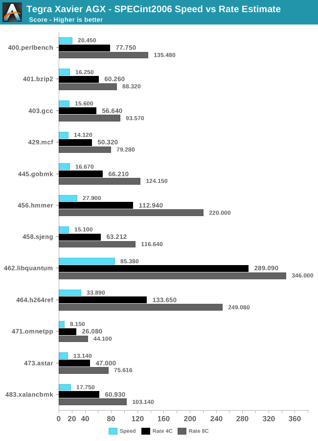
The way that SPEC2006 rate scores are calculated is that it measures the execution time of all instances and uses the same reference time scale as the Speed score- with the only difference here being is that the final score is multiplied by the amount of instances.
I chose to run the rate benchmarks with both 4 and 8 instances to showcase the particularity of NVIDIA’s Carmel CPU core configuration. Here we see the four core run perform roughly as expected, however the eight core run scores are a bit less than you’d expect. To showcase this better, let’s compare the scaling factor in relation to the single-core Speed results:
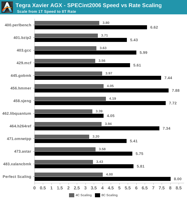
The majority of the 4C workloads scaling near the optimal 4x factor that we’d come to expect, with only a few exceptions having a little worse performance scaling figures. The 8C workloads however showcase significantly worse performance scaling factors, and it’s here where things get interesting:
Because Xavier’s CPU complex consists of four CPU clusters, each with a pair of Carmel cores and 2MB L2 cache shared among each pair, we have a scenario where the CPU cores can be resource constrained. In fact, by default what the kernel scheduler on the AGX does is to try to populate one core within all clusters first, before it schedules anything on the secondary cores within a cluster.
In effect what this means that in the 4C rate scenarios, each core within a cluster essentially has exclusive use of the 2MB L2 cache, while on the 8C rate workloads, the L2 cache has to be actively shared among the two cores, resulting in resource contention and worse performance per core.
The only workloads that aren’t nearly as affected by this, are the workloads which are largely execution unit bound and put less stress on the data plane of the CPU complex, this can be seen in the great scaling of some workloads such as 456.hmmer for example. On the opposite end, workloads such as 462.libquantum suffer dramatically under this kind of CPU setup, and the CPU cores are severely bandwidth starved and can’t process things any faster than if there were just one core per cluster active.
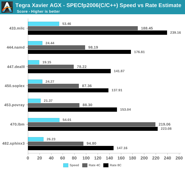
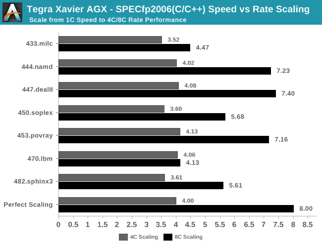
The same analysis can be applied to the floating point rate benchmarks: Some of the less memory sensitive workloads don’t have all that much issue in scaling well with core counts, however others such as 433.milc and 470.lbm again showcase quite bad performance figures when run on all cores on the system.
Overall, NVIDIA's design choices for Xavier’s CPU cluster are quite peculiar. It’s possible that NVIDIA either sees a majority of workloads targeted on the AGX to not be an issue in terms of their scaling, or actual use of the platform in automotive use-cases we would see each core in a cluster operating in lock-step with each other, theoretically eliminating possible resource contention issues on the level of the shared L2 cache.
I didn’t get to measure full power figures for all rate benchmarks, but in general the power of an additional core within a separate cluster will scale near linearly with the power figures of the previously discussed single-core Speed runs, meaning the 4-core rate benchmarks showcase active power usage of around ~12-15W. Because performance doesn’t scale linearly with the additional secondary cluster cores, the power increase was also more limited. Here I saw up to a total system power consumption of up to ~31W for workloads such as 456.hmmer (~22W active), while more bottlenecked workloads ran around ~21-25W for the total platform (~12-16W active).


51 Comments
View All Comments
linuxgeex - Friday, November 8, 2019 - link
Add this line to the following files (linux/bsd or windows)/etc/hosts or c:/windows/system32/driver/hosts
127.0.0.1 ads.servebom.com
job done.
TheinsanegamerN - Friday, January 4, 2019 - link
auto video ads are hell incarnate.Yojimbo - Friday, January 4, 2019 - link
Regarding NVIDIA's future CPU core development, I think it's important to note that NVIDIA has developed all major IP blocks on the SoC. That probably allows them to work on integration sooner than if they relied on externally developed IP blocks. Also, they have the ability to tune their cores and fabric to their intended application, which is a narrow subset of what ARM is developing for. I'm guessing NVIDIA doesn't tune the performance of their CPU cores using specint or specfp. They probably look at much more specific and realistic benchmarks.And by the time the Cortex A76AE is available for NVIDIA to use they will probably have a next iteration of their CPU which perhaps will show up in Orin in early 2021 or even late 2020. It's not clear to me what delayed Xavier from NVIDIA's original schedule. It's possible they'll be able to get the next one out with less time between the launch of the underlying GPU architecture and the availability of the SoC. There was a lot of new stuff that went into Xavier other than the GPU architecture, such as the increased safety features, the DLA, and the PVA.
DeepLearner - Friday, January 4, 2019 - link
I hope they'll send you a T4 soon! I'm dying for numbers on those.eastcoast_pete - Friday, January 4, 2019 - link
@Andrei: thanks for this review. I wonder if the recent loss of a larger client in the automotive sector (Audi/Volkswagen) to Samsung played a role in Nvidia's willingness to make samples available to you for review. As of model year 2021, Audi will stop using Tegra-based units and move to Samsung's Exynos Auto V9 SoC, which actually features an 8 A76 cores based on ARM's A76 AE design for automotive/vehicular use.While that specialized SoC is still awaiting mass production, I also wonder if Samsung's choice to use straight-up ARM A76 cores (yes, they are AE, so not standard A76) portends a sea change for the mainstream Exynos lines also? As you pointed out, Mongoose turned out to be quite disappointing, so is there a change coming? Would appreciate your insights and comment!
webdoctors - Friday, January 4, 2019 - link
I was also confused by the news of Audi using Samsung chips. I don't think this changes the Audi/Nvidia relationship from googling: http://fortune.com/2017/01/05/audi-nvidia-2020/I think in the infotainment sector there's just a lot of competition for cheap chips and a low bar for entry. Any Mediatek or run of the mill cellphone chip should do. I doubt you'd care about ECC or safety in the HW playing your music or watching movies. My current car has an aftermarket unit that's 10 years old that can play DVD movies, has GPS maps and integrates a backup camera.
I'm not sure how you'd program a beast of a chip here, or even what the right benchmarks are since you wouldn't need it just play movies, show maps or run CPU benchmarks. With all the inferencing and visual processing it'd be a waste of resources and money to use it for the traditional tasks done today in cars.
I'm really curious how Anandtech evaluates these specialized products that aren't your run of the mill CPU/GPU/HDD.
unrulycow - Saturday, January 5, 2019 - link
This is obviously overkill for the entertainment system. It's main purpose is for the semi-autonomous driving systems like Cadillac's SuperCruise or Tesla's Autopilot.Andrei Frumusanu - Friday, January 4, 2019 - link
As far as I know their mobile roadmap still uses custom cores, there's probably different requirements for automotive or they could have simply said that 8 A76s make a lot more sense than 8 custom cores.eastcoast_pete - Saturday, January 5, 2019 - link
Thanks Andrei! Yes, design requirements for automotive/vehicle-embedded are different in key areas (safety/security). However, I was/am struck by Samsung not adapting their own Mongoose design for AE use. Maybe their client (Audi) preferred the stock A76 AE design, and it wasn't economical to adapt Mongoose. However, this now means that the most powerful Samsung SoC design (A76 octacore) might be found in - Audi cars.unrulycow - Saturday, January 5, 2019 - link
They are also losing Tesla as a client. Tesla decided to create their own chip which will theoretically start going into cars in Q2. I would love to see a comparison between the two chips.