Intel's 10nm Cannon Lake and Core i3-8121U Deep Dive Review
by Ian Cutress on January 25, 2019 10:30 AM ESTStock CPU Performance: Legacy Tests
We have also included our legacy benchmarks in this section, representing a stack of older code for popular benchmarks.
All of our benchmark results can also be found in our benchmark engine, Bench.
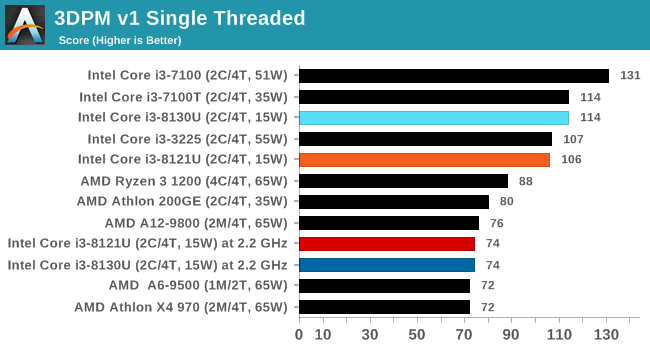
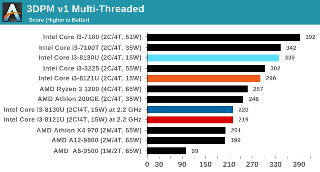
3DPM v1: Naïve Code Variant of 3DPM v2.1
The first legacy test in the suite is the first version of our 3DPM benchmark. This is the ultimate naïve version of the code, as if it was written by scientist with no knowledge of how computer hardware, compilers, or optimization works (which in fact, it was at the start). This represents a large body of scientific simulation out in the wild, where getting the answer is more important than it being fast (getting a result in 4 days is acceptable if it’s correct, rather than sending someone away for a year to learn to code and getting the result in 5 minutes).
In this version, the only real optimization was in the compiler flags (-O2, -fp:fast), compiling it in release mode, and enabling OpenMP in the main compute loops. The loops were not configured for function size, and one of the key slowdowns is false sharing in the cache. It also has long dependency chains based on the random number generation, which leads to relatively poor performance on specific compute microarchitectures.
3DPM v1 can be downloaded with our 3DPM v2 code here: 3DPMv2.1.rar (13.0 MB)
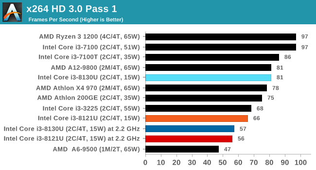
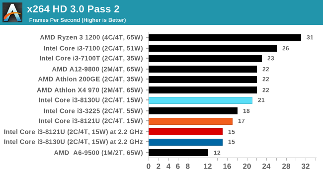
x264 HD 3.0: Older Transcode Test
This transcoding test is super old, and was used by Anand back in the day of Pentium 4 and Athlon II processors. Here a standardized 720p video is transcoded with a two-pass conversion, with the benchmark showing the frames-per-second of each pass. This benchmark is single-threaded, and between some micro-architectures we seem to actually hit an instructions-per-clock wall.


129 Comments
View All Comments
yeeeeman - Saturday, January 26, 2019 - link
As someone said it earlier in this thread, I think we miss opportunities when moving to a new process every two years. The mishap that Intel had just showed us how much better a process can become if you give the time to your engineers. 14nm started late, with some low clocked parts. We had some Broadwell chips that ran at 3.3 base. Then, Skylake came and the 6700k brought 4ghz at quite high power. Then, the 7700k came and another tweak to the process improved clocks, so we now got 4.7 GHz boost. After this, things moved up in core counts (which should've happen a long time ago, but with competition...) and we got 8700k and now 9900k with turbo to 5ghz. Until now, only 32nm with Sandy Bridge came close to 5ghz mark. Now, with a lot of time to tweak, they have become so confident in the 14nm process that they released a 5ghz stock cpu. Financials say the true story. Even if we cry about 10nm, truth is that things can move forward without a new process. It is cheaper actually to prolong the life of a certain process and if they can add enough improvements from generation to generation, they can afford to launch new process once every 4-5 years.Dodozoid - Saturday, January 26, 2019 - link
Indeed, we probably have to get used to a lot of +++ processes. During the architecture day, the new Intel people (old AMD people) mentioned they are decoupling the architecture from the process. That means they can make progress other than pushing clocks on the same core over and over, but IPC as well...KOneJ - Sunday, January 27, 2019 - link
Unfortunately, SB-derivatives seem to be needing a significant overhaul. "tocks" of late haven't exactly brought meaningful IPC gains. Hopefully deeper and wider *Cove designs are a step in the right direction. I just don't like that Intel seems to be taking an approach not dissimilar to the Pentium 4 the last time AMD reared its head. Only this time, a major departure in micro-architecture and steady process advantage isn't in the wings. Even with the *Coves, I think AMD may be able to build enough steam to solidly overtake them. There's no reason that Zen 4 and on couldn't go deeper and wider too, especially looking at power consumption on the front and back ends of the Zen core versus the uncore mesh. I think Zen derivatives currently will try the wider first. It actually might make the high core-count parts significantly more power efficient. Also could easily scale better than post-SB did if Agner Fog's analysis is anything to go by. Multiple CPU die masks and uncore topologies incoming? Wouldn't surprise me.dgingeri - Saturday, January 26, 2019 - link
Well, yeah, they can be improved upon over time, but that doesn't cut the production costs like a process reduction does. improving the process can increase yields and increase performance, but only by a limited percent. A process reduction increases the number of chips from a wafer by a much higher amount, even if there are more defects.Well, that was the way it worked up until the 14nm process.
With 10nm at Intel, they had far too many defects, and the process failed to give the returns they wanted for quite a while. That had as much to do with the quality of the wafers before production as it did the production process itself. They had to push the wafer producers to higher levels of purity in order to fix that. I'm fairly sure TSMC would have had the same issues with their 7nm, but Intel had already pushed the wafer production to higher levels of purity because of their problems, so TSMC was able to take a couple extra steps ahead because of that.
These days, we're going to see each step smaller take longer and longer to get right, because of these same hurdles. As things get smaller, impurities will have a higher and higher impact on production. We may not get as far as some are hoping, simply because we can't get silicon as pure as necessary.
name99 - Saturday, January 26, 2019 - link
"Another takeaway is that after not saying much about 10nm for a while, Intel was opening up. However, the company very quickly became quiet again."The history page is great. But I have to wonder if the ultimate conclusion is that the best thing, for both Intel and the world, is that they STICK to the STFU strategy? And that journalist stick to enforcing it.
One thing that's incredibly clear from all this is that Intel are utterly lousy at forecasting the future. Maybe it's deliberate lies, maybe it's just extreme optimism, maybe it's some sort of institutional pathology that prevents bad news flowing upward?
Regardless, an Intel prediction for beyond maybe two years seems to be utterly worthless. Which raises the question -- why bother asking for them, and why bother printing them?
Look at that collection of technologies from the 2010 slide that are supposed to be delivered over the next nine years. We got Computational Lithography, and that's about it. CErtainly no III-V or Germanium or Nanowires. Interconnects (Foveros and EMIB?) well, yeah, in about as real a form as 10nm. 3D refers to what? Die stacking? or 3D structures? Either way nothing beyond the already extant FinFETs. Dense Memory? Well yeah, there's Optane, but that's not what they had in mind at the time, and Optane DIMMs are still crazy specialized. Optical Interconnect? Well occasional mutterings about on-die photonics, but nothing serious yet.
Now on the one hand you could say that prediction is hard. How much better would IBM, or TSMC, or Samsung, have done? On the other hand (and this is the point) those companies DON'T DO THIS! They don't make fools of themselves by engaging in wild claims about what they will be delivering in five years. Even when they do discuss the future, it's in careful measured tones, not this sort of "ha ha, we have <crazy tech> already working and all our idiot competitors are four years behind" asinine behavior.
I suspect we'd all be better off if every tech outlet made a commitment that they won't publish or discuss any Intel claims regarding more than two years from now. If you're willing to do that, you might as well just call yourself "Home of Free Intel's advertising". Because it's clear that's ALL these claims are. They are not useful indications of the future. They're merely mini-Intel ads intended to make their competition look bad, and with ZERO grounding in reality beyond that goal.
KOneJ - Sunday, January 27, 2019 - link
While you're correct that the media is ignorantly doing just that for the most part, at least this article provides context in what Intel is trying to do in obfuscating the numbers versus TSMC and Samsung who haven't stumbled the same way. Some of the Foveros "magic" is certainly not being knocked-down enough when people don't understand what it's intended to do. 2.5D, 3D, MCMs, and TSVs all overlap but cover different issues. I blame the uneducated reader more than anything. Good material is out there, and critical analysis between the lines is under-present. "Silicon photonics" was a big catch-phrase in calls a few years ago, but quiet now. Hype, engineering, and execution are all muddied by PR crap. Ian is however due credit for at least showing meaningful numbers. It's more in the readers hands now. Your last remarks really aren't fair to this article, even if they bear a certain degree of merit in general. Sometimes lies are needed to help others understand the truth though...HStewart - Saturday, January 26, 2019 - link
I believe that this Cannon is get AVX 512 out to developers. What would be interesting if possible is for Intel to release Covey Lake on both 14nm and new 10nm. One thing I would expect that Covey Lake will significant speed increase compare to current 14nm chips even if on 14nm and the 10nm will be also increase but combine Covey Lake and new 10nm+. should be quite amazing.One test that I am not sure is benchmark that runs in both AVX2 and AVX 512 and see the difference. There must be reason why Intel is doing the change.
KOneJ - Sunday, January 27, 2019 - link
Cheap Cannon Lake is not designed to get AVX512 into dev hands. That's the dumbest thing ever. And "Covey Lake"? Please read the article before commenting. There are a few good blog posts and whitepapers out there analyzing and detailing SIMD across AVX varieties. For most things, AVX512 isn't as big a deal as earlier SIMDs were. It has some specialized uses as it is novel, but vectoring code and optimizing compilers to maturity is slow and difficult. There are fewer quality code slingers and devs out there than you would expect. Comp sci has become littered with an unfortunate abundance of cheap low-quality talent.HStewart - Sunday, January 27, 2019 - link
Ok for the misunderstood people about AVX 512 - which appear to be 2x fast AVX2https://www.prowesscorp.com/what-is-intel-avx-512-...
yes it going to take a while people user AVX 512 - but just think about it twice the bits - I was like you not believe 512 but instead 64 bit would make in days of early 64 bit - thinking primary that is will make program largers and not necessary. As developer for 3 decades one thing I have send that 64 bit has done is make developer lazy - more memory less to worry about in algorithms for going to large arrays.
As for Sunny Cove, it logical with more units in the chip - it is going to make a difference - of course Cannon Lake does not have Sunny Cove - so it does not count. Big difference will be seen when Covey Lake cpus come out what the difference it be like with Cannon Lake - and even Kaby Lake and assoicated commetitors chips
HStewart - Sunday, January 27, 2019 - link
One thing on Covey Lake and upcoming 7nm from Intel, it is no doubt that it designers made a mistake with Cannon Lake's 10nm - Intel realizes that and has created new fabs and also new design architexture - there is no real reason for Intel to release a Cannon Lake - but it good to see that next generation is just more that Node change - it includes the Covey Lake architexture change.