Hot Chips 2018: Samsung’s Exynos-M3 CPU Architecture Deep Dive
by Andrei Frumusanu on August 20, 2018 1:00 PM ESTPhysical Layout: Making Sense of the Silicon Blocks
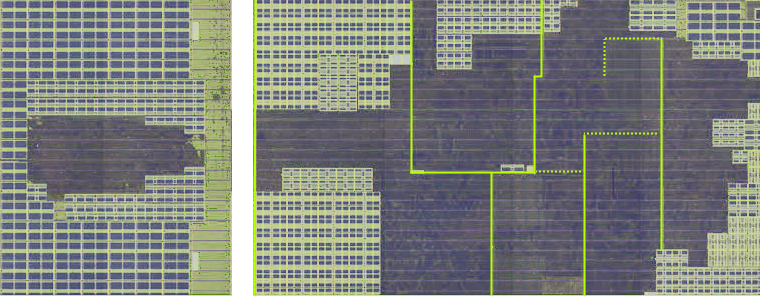
 Exynos M1 Core Layout

Exynos M3 Core Layout
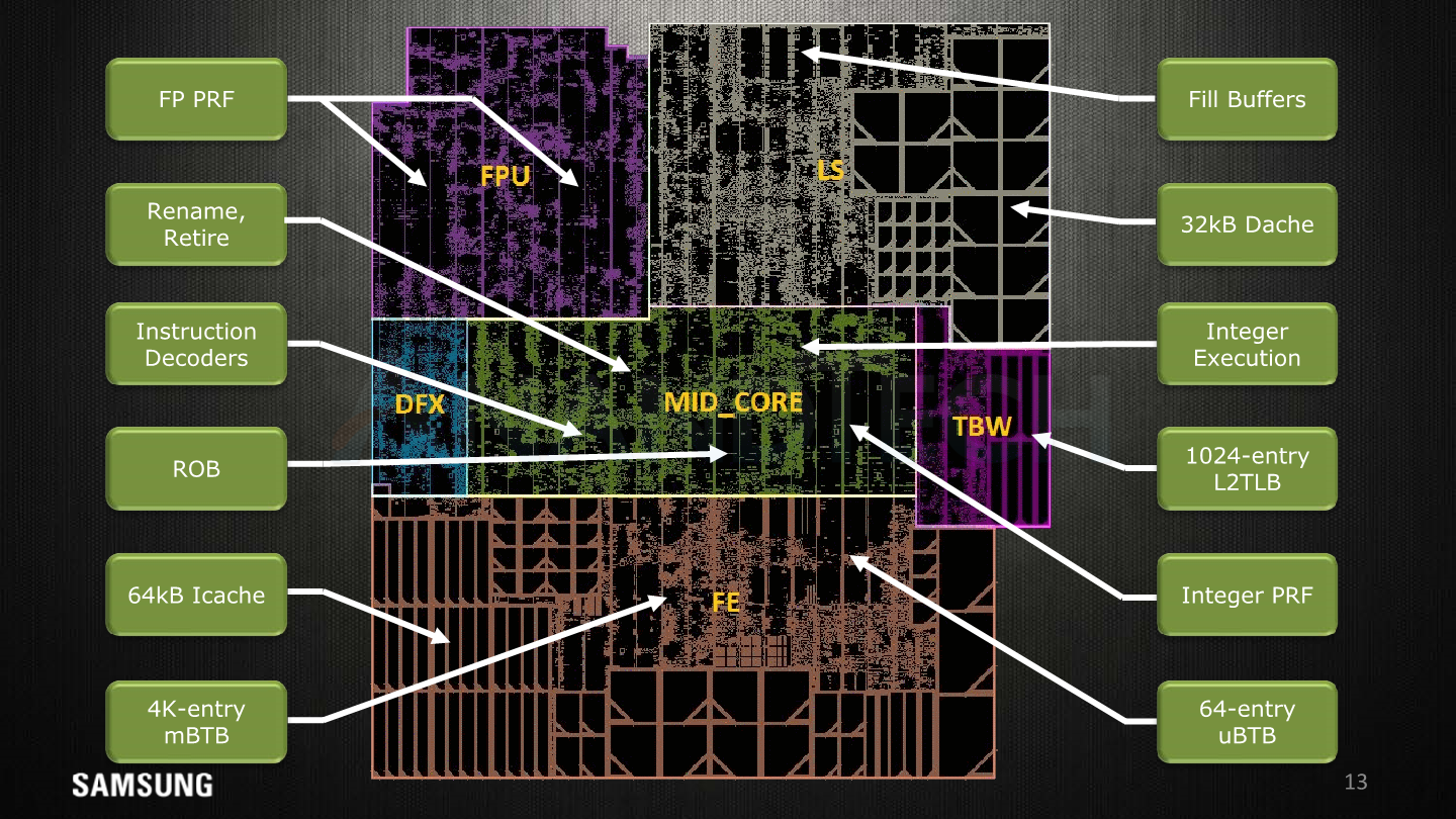
Samsung delights us with this disclosure this year, as they break down the core’s floor plan in this slide. I’m pretty happy to have been almost accurate with the medium resolution die shot I had at hand in delimiting the various function blocks in the original review article.
Here’s some short explanations on the terms:
- pL2: Private L2 cache, here we see the 512KB cache implemented in what seems to be two banks/slices.
- FPB: Floating point data path; the FP and ASIMD execution units themselves.
- FRS: Floating point schedulers as well as the FP/vector physical register file memories.
- MC: Mid-core, the decoders and rename units.
- DFX: This is debug/test logic and stands for “design for X” such as DFD (Design for debug), DFT (Design for test), DFM (Design for manufacturability), and other miscellaneous logic.
- LS: Load/store unit along with the 64KB of L1 data cache memories.
- IXU: Integer execution unit; contains the execution units, schedulers and integer physical register file memories.
- TBW: Transparent buffer writes, includes the TLB structures.
- FE: The front-end including branch predictors, fetch units and the 64KB L1 instruction cache memories.
Exynos 9810 Floor Plan. Image Credit TechInsights
Overall compared to the M1, almost all facets of the functional units in the M3 have vastly increased in size. The end product ends up at 2.52mm² for the core’s functional blocks, plus another 0.98mm² for the 512LB L2 cache and logic.
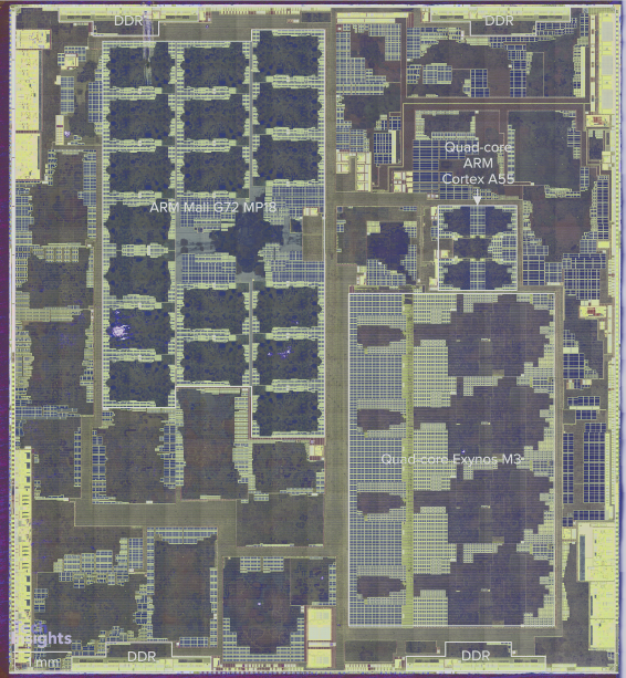
Exynos 9810 Floor Plan. Image Credit TechInsights
Here Samsung showcases the whole cluster floorplan, again marking the 4 cores laid down next to each other in a row with the L2 and L3 slides also orderly placed next to each other. This layout seems to have saved some layout efforts as each block is designed once and then simply replicated 4 times.
59% Higher IPC Across Variety of Workloads

Finally Samsung talks a bit about their performance profiling infrastructure and how they run various amounts of workload traces through the RTL and model simulators in order to evaluate design choices, find mistakes, and do fine-tuning to the µarch.
In this slide we finally have an official figure for the IPC increase for the core: ~59%. I had pointed out at >50% at the beginning of the year, so I'm glad to see that work out in the end. As we see in the graph, the increase is naturally not linear across all workloads and we see limited increases of only 25% in high ILP workloads, to near to not much of an increase in what is likely to be MLP workloads. Conversely, there’s also a lot of mixed workloads where the IPC increase is >80%.
Performance & Efficiency: Samsung's Data and AnandTech's Data
The next slides showcase a snippet of the performance improvements on GeekBench4 between the M2, M3, and the A75; representing commercial performance on the Exynos 8895, Exynos 9810 and the Snapdragon 845.
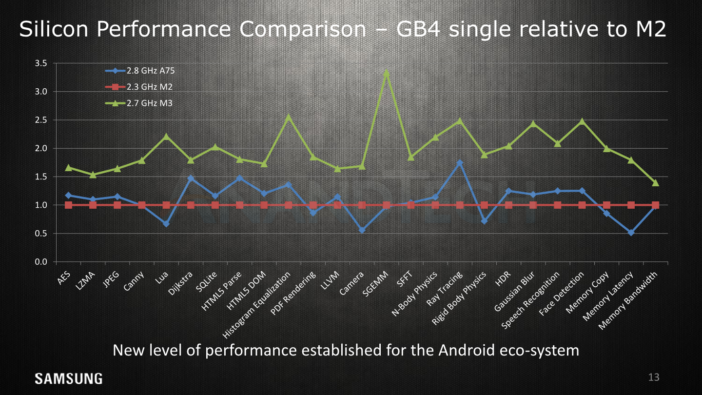
Again we’ve already very much extensively covered the performance aspects of the SoC and microarchitecture in past articles;
- The Samsung Galaxy S9 and S9+ Review: Exynos and Snapdragon at 960fps
- Improving The Exynos 9810 Galaxy S9: Part 1
- Improving The Exynos 9810 Galaxy S9: Part 2 - Catching Up With The Snapdragon
To add to today’s µarchitecture article I’m also adding some new SPEC scores which improve on the originally review data. The difference and cause for the improvement is DVFS tweaking, further scheduler enhancements, and a more synthetic testing environment and care with coping with the higher power draw at the M3’s maximum frequencies.

Click for large full resolution
I won’t go over the details of the scores, but the performance improvements under the new conditions more closely represents the kind of high jump Samsung showcases in GB4.
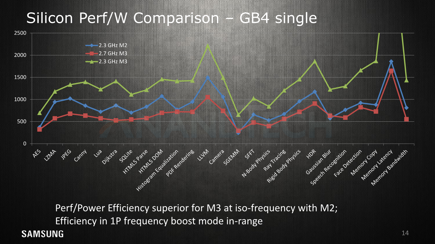
Power efficiency has been a big topic for the M3 – and here it is quite telling that they chose to omit results of competing solutions. As we’ve covered in our reviews, Samsung’s high boost clock at up to 2.7GHz comes at a price of very high required voltages and exponential power draw. Here, even though it showcases leading edge performance, it ends up less efficient than the Exynos 8895’s M2. The figures here represent active system power; that means CPU, memory controller, DRAM, much in the same way we measure it here at AT.
Reducing the clock to the same 2.3GHz as the M2, we see the M3 lead in terms of efficiency as per Samsung’s presentation.
To add to Samsung's data and give more context, I’m reposting the revised benchmark and efficiency overview in our own independently performed analysis of the platform. The below chart showcases the energy usages to finish the workload suite, alongside the average power consumption during the test. The left bars represent the consumed energy in Joures, and the shorter the bars are (the less energy), the more efficient a platform is. The right bars represent the performance score, the longer the bars denoting better performance.
I’ve also re-tested the workloads at the three top-frequencies of the M3; 1794, 2314 and 2704MHz, giving us a wider idea of how the efficiency scales with performance.

Overall the M3 offers a quite dynamic range in its results. At (almost) equivalent peak performance against the competing A75 results for this generation, the M3 is able to post a good efficiency advantage. This lower performance point of the M3 still outperforms the 2.3GHz maximum performance of the M2 – all while having significant power and energy efficiency advantages.
Clocking it up to 2.3GHz here the M3 more clearly outperforms the A75, albeit at an efficiency hit in the integer workloads, while the FP workloads closely match the Arm competition.
Finally the 2.7GHz results further the performance gap, but comes at a great cost in efficiency, using up more energy than any other recent SoC.
The fact that the E9810 had a cluster of 4 M3 cores running on the same frequency and voltage plane came at a cost of overall efficiency. Secondary threads that didn’t require the peak performance driven by a larger primary thread, but whose requirements are still bigger than the capacity of the littles cores, had to take a large the efficiency hit of running at the same bad efficiency points as the biggest thread in the cluster. The result of this adds to the bad battery life scores we’ve come to measure.
I’ve been able to resolve the scheduling issues in a custom kernel, improving the web browsing score further to 9h, however there are still compromises that just can’t be resolved due to how the SoC operates. Here I expect Samsung to depart from the 4 “huge core” topology for the next generation M4 and introduce something that will be a lot more power efficient in diverse multi-threaded scenarios.


45 Comments
View All Comments
eastcoast_pete - Tuesday, August 21, 2018 - link
Knowing that this might rub some here the wrong way: While I agree that the style and grammar of Andrei's article could have been improved by an editor or proofreader, I mainly read articles here at Anandtech for their content, not style or grammar. As far as I can tell, Andrei's article was not littered with wrong or confusing statements or facts; conversely, it was an (obviously) quickly written, yet accurate summary of a very recent presentation at Hot Chips with some helpful background added.So, while I agree that a quick proofreading, preferably by another pair of eyes, would have
likely avoided some issues, I for one prefer high quality, accurate breaking news in occasionally imperfect English over perfect prose with missing or wrong facts and weeks late.
So, can we get back to the technology, which is what brings us here?
Speedfriend - Wednesday, August 22, 2018 - link
Exactly, if you don't like the grammar or style, go somewhere else...and stop being pedanticjospoortvliet - Wednesday, August 29, 2018 - link
Agreed. His articles are among the very best in terms of technical detail yet clarity and that is all I care for.abufrejoval - Friday, August 24, 2018 - link
As you hint, the power consumption disadvantages might not be as significant in a bigger form factor, such as an Slimbook (can't say Ultrabook, right?) or a tablet. Even the Kirin 950 (or was it 960?) which burned way too much in a phone seems to be adequate enough in tablets, where the larger displays tend to offset what the SoC eats in batteries.I
abufrejoval - Friday, August 24, 2018 - link
wonder if they'd sell suprplus chips cheap :-)want edit!