Hot Chips 2018: Samsung’s Exynos-M3 CPU Architecture Deep Dive
by Andrei Frumusanu on August 20, 2018 1:00 PM ESTSamsung's Future Strategy & Conclusion
Lastly, Samsung talks more about the project’s timelines and how things got put into motion. As we discussed in the introduction, the M3’s planning was kicked off in 2Q14 with RTL start in 1Q15, following the completion of the M1. During this time, Samsung had a change of cadence and planning, forking a subset of features originally planned for the M3 and putting them in into the M2 in 3Q15. Here the original M3’s plans were revised for a bigger microarchitecture push for performance in the first quarter of 2016.
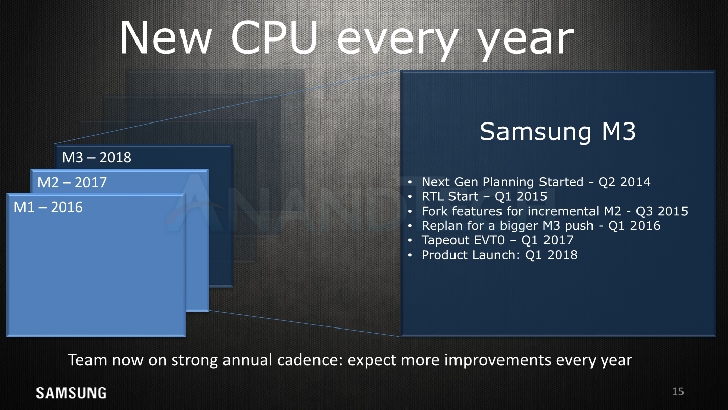
The RTL was handed off to the SoC team in 1Q2017 for the first EVT0 tapeout of the Exynos 9810. It’s to be noted that actual production silicon is EVT1, whose tape-out happened sometime in the middle of 2017. Finally the Exynos 9810 saw commercial availability in March 2018.
The M3 is said to have been quite a sweat-breaking effort for the design team, having to have gone through what seems to have been a major replanning of the project, and having to deal with extreme time-pressure in terms of hitting a hard deadline in order to make it into the next generation product.
Here it seems Samsung still left a lot of improvements on the table that didn’t make it into the M3 due to time constraints. The cache hierarchy in particular what seems to be one of the weaker parts of the microarchitecture, which is something Samsung admits they aren’t quite happy with. It was one of the features that pushed the design team hard in order to make out the door in time.
One aspect that Samsung didn’t, and wasn’t willing to talk about, is any kind of physical implementation details. As HotChips is a microarchitecture forum, the disclosures were kept to the µarch of the M3. As we’ve seen in the past, a single microarchitecture can end up quite differently in its performance and power characteristics when implemented differently by vendors. Taking this into account, when measuring the end-product, it’s hard to separate these intertwined aspects of a piece of silicon.
The M3 seems like an overall solid microarchitecture which feels a lot more like what we see in desktop grade products. It also feels like Samsung took a more straightforward approach in terms of leveraging performance out of the µarch – in many aspects it’s just a much bigger beast than what we see from Arm – and thus also explains the M3’s quite large silicon size.
When evaluating efficiency of a piece of IP, looking at the higher-level microarchitecture is not enough, and here aspects of the actual electrical engineering of the transistor structures and details in their design choices can easily outweigh any apparent higher level characteristics. Here we’re largely out of our depth and no vendors will really ever make disclosures of such detail, not to mention it would be vastly out of scope for public readerships.
Here the final slide contains probably the most revealing disclosure that gives us a glimpse of Samsung’s future strategy: the SARC design team is said to now be on a strong annual release cadence with continued improvements every year. Indeed when I was making comparisons between the M3 and A76 in asking about some different design choices and specifications, Samsung didn’t shy in reminding me that the real competition for Arm’s new core will be next year’s new Exynos M4, not the M3.
We’ve only had two generational improvements released to date, but with 20% and 59% in IPC gains for the M2 and M3, Samsung does post an albeit short, but very robust track-record. Only just days ago Arm publicly announced its performance core roadmap through to 2020, revealing A76 successors Deimos and Hercules, promising ~15% and 10% generational gains. Here the M3 already seems to match or exceed the A76 in projected performance (at least in SPEC2006), so depending on the power efficiency of the M4, we might finally see a competitive advantage pay-off for Samsung’s custom designs.
Overall, we do thank Samsung for doing microarchitectural disclosures such as seen today, as beyond Arm’s own products, they are a quite a rare event in the ever so secretive industry. Here’s to hoping S.LSI and SARC resolve the Exynos 9810 and M3’s weaknesses and are pushing hard to make next year’s SoC a larger success. We’ll definitely looking forward to get our hands on it!


45 Comments
View All Comments
HStewart - Monday, August 20, 2018 - link
One thing I curious is why does Samsung use this CPU in Europe products and use SnapDragon in US, Japan Markets - Only thing I can think of regulations for security on the chips.Great_Scott - Monday, August 20, 2018 - link
My understanding is that the US version uses the SnapDragon for the integral modem.I'm not exactly sure why this is, it might be an artifact of needing legacy CDMA support for Verizon/Sprint, which isn't needed for a world-phone.
beginner99 - Tuesday, August 21, 2018 - link
That is what I thought as well. CDMA. Not needed for rest of the world.abufrejoval - Friday, August 24, 2018 - link
Unless you assume that some people actually travel. You might even argue that the average European is more likely to enter CMDA space in his life-time than the other way around: Most US citizens only ever leave the country to fight a war, I keep hearing.I prefer to chose myself than have choices mandated to me based on where I tend to be most of the time.
Ej24 - Friday, August 24, 2018 - link
Samsungs own Shannon modem works on CDMA. My galaxy S6 on Verizon Wireless is proof of that. It's probably legal reasons, patents, licensing whatever. It's annoying. Because the Qualcomm has put out some duds and we don't have a choice.az060693 - Monday, August 20, 2018 - link
It's supposedly due to a 1993 patent licensing deal- https://www.androidcentral.com/qualcomm-licensing-...Though in certain phone generations, it might have also been to supply issues.
HStewart - Monday, August 20, 2018 - link
That sounds about right - but I believe the Qualcomm version is faster than the Samsung version. This is a problem with have Modem built into chip - you have to used different CPU depending on which modem is in the SOC,bebby - Tuesday, August 21, 2018 - link
There is another more or less official reason - to reduce risks - instead of only relying on one chip, they use 2, one in-house designed and one external, in case the internal chip has issues. Samsung anyhow manufactures both in-house.name99 - Monday, August 20, 2018 - link
At least one reason they use Snapdragon is for markets that still require voice CDMA, which QC modems provide.aryonoco - Monday, August 20, 2018 - link
The S6 showed that Samsung has no problems making integrated CDMA modems.