Hot Chips 2018: Samsung’s Exynos-M3 CPU Architecture Deep Dive
by Andrei Frumusanu on August 20, 2018 1:00 PM ESTSamsung's Future Strategy & Conclusion
Lastly, Samsung talks more about the project’s timelines and how things got put into motion. As we discussed in the introduction, the M3’s planning was kicked off in 2Q14 with RTL start in 1Q15, following the completion of the M1. During this time, Samsung had a change of cadence and planning, forking a subset of features originally planned for the M3 and putting them in into the M2 in 3Q15. Here the original M3’s plans were revised for a bigger microarchitecture push for performance in the first quarter of 2016.
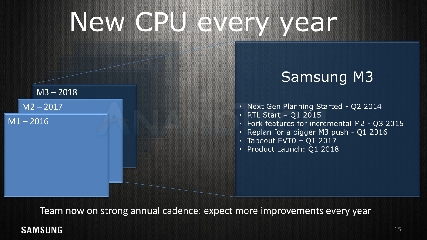
The RTL was handed off to the SoC team in 1Q2017 for the first EVT0 tapeout of the Exynos 9810. It’s to be noted that actual production silicon is EVT1, whose tape-out happened sometime in the middle of 2017. Finally the Exynos 9810 saw commercial availability in March 2018.
The M3 is said to have been quite a sweat-breaking effort for the design team, having to have gone through what seems to have been a major replanning of the project, and having to deal with extreme time-pressure in terms of hitting a hard deadline in order to make it into the next generation product.
Here it seems Samsung still left a lot of improvements on the table that didn’t make it into the M3 due to time constraints. The cache hierarchy in particular what seems to be one of the weaker parts of the microarchitecture, which is something Samsung admits they aren’t quite happy with. It was one of the features that pushed the design team hard in order to make out the door in time.
One aspect that Samsung didn’t, and wasn’t willing to talk about, is any kind of physical implementation details. As HotChips is a microarchitecture forum, the disclosures were kept to the µarch of the M3. As we’ve seen in the past, a single microarchitecture can end up quite differently in its performance and power characteristics when implemented differently by vendors. Taking this into account, when measuring the end-product, it’s hard to separate these intertwined aspects of a piece of silicon.
The M3 seems like an overall solid microarchitecture which feels a lot more like what we see in desktop grade products. It also feels like Samsung took a more straightforward approach in terms of leveraging performance out of the µarch – in many aspects it’s just a much bigger beast than what we see from Arm – and thus also explains the M3’s quite large silicon size.
When evaluating efficiency of a piece of IP, looking at the higher-level microarchitecture is not enough, and here aspects of the actual electrical engineering of the transistor structures and details in their design choices can easily outweigh any apparent higher level characteristics. Here we’re largely out of our depth and no vendors will really ever make disclosures of such detail, not to mention it would be vastly out of scope for public readerships.
Here the final slide contains probably the most revealing disclosure that gives us a glimpse of Samsung’s future strategy: the SARC design team is said to now be on a strong annual release cadence with continued improvements every year. Indeed when I was making comparisons between the M3 and A76 in asking about some different design choices and specifications, Samsung didn’t shy in reminding me that the real competition for Arm’s new core will be next year’s new Exynos M4, not the M3.
We’ve only had two generational improvements released to date, but with 20% and 59% in IPC gains for the M2 and M3, Samsung does post an albeit short, but very robust track-record. Only just days ago Arm publicly announced its performance core roadmap through to 2020, revealing A76 successors Deimos and Hercules, promising ~15% and 10% generational gains. Here the M3 already seems to match or exceed the A76 in projected performance (at least in SPEC2006), so depending on the power efficiency of the M4, we might finally see a competitive advantage pay-off for Samsung’s custom designs.
Overall, we do thank Samsung for doing microarchitectural disclosures such as seen today, as beyond Arm’s own products, they are a quite a rare event in the ever so secretive industry. Here’s to hoping S.LSI and SARC resolve the Exynos 9810 and M3’s weaknesses and are pushing hard to make next year’s SoC a larger success. We’ll definitely looking forward to get our hands on it!


45 Comments
View All Comments
name99 - Wednesday, August 22, 2018 - link
The issue is not technology (everyone knows CDMA basics because you need it on the data side for WCDMA aka 3G). The issue is licensing.Maybe QC changes the licensing terms so that doing it in-house was simply not worth the cost? This seems very much in-line with the world-wide lawsuits against QC for various anti-competitive behavior.
petar_b - Saturday, November 3, 2018 - link
I when they use Exynos they have less royalty fees to pay since it's their own processor. EU market is smaller than the US or ASIA so they compensate by providing chip with cheaper costs.PS - CDMA, modem and all other reasons mentioned are irrelevant; other brands use Qualcom in EU and all works perfectly.
AlB80 - Monday, August 20, 2018 - link
Unused cores do not consume energy at all regardless of voltage. Thus there should be two threads on performance cores, one requires 3 GHz, but second do not, to lose efficiency.linuxgeex - Tuesday, August 21, 2018 - link
While technically you're right that the core itself doesn't draw power when it's powered down, there's other factors to consider:1) the power cost to power it down and back up when you need it again. If you use the core intermittently then the cost of powering it up and down can exceed the cost of operating it for the workload, and then it may be more efficient to keep those jobs on the less efficient core(s)
2) the uncore, ie the busses and support logic that don't get powered down, can use nearly as much power as the cores themselves. In some CPUs, ie Ryzen2 TRW 2990WX the uncore actually consumes 76% of the die power when there's only 2 cores out of 32 active.
name99 - Monday, August 20, 2018 - link
"When Arm disclosed the A76 µarch details and particularly the 128-entry ROB (which in comparison seems quite small to the M3), they said that this was a balance between performance and area/power. In particular we saw a mention that a 7% increase in the ROB capacity only came with a 1% performance gain on average."ROB per se costs very little, it's just a queue.
What is expensive is the physical register file, and the fact that it more or less scales with the size of the ROB (since most instructions generate one value, which consumes one physical register).
The trick, then, is what can you do to increase the size of the ROB (which allows you to do more work during dead periods while your ROB-blocking instruction at the head of the queue is waiting on DRAM) without paying the cost of the register file?
There is a bag of tricks for this, and as you make your CPU more advanced, you use more and more of them. They include
- clustering (so you duplicate the register file, and have half the execution units use one of the register files, the other half use the other register file. This works because there are quadratic aspects to the register file, so cutting some things in half [even if they are then duplicated] reduces area/power by four.
- various "resource amplification" techniques getting more use out of what you have. These might be giving your register file one fewer read ports, but then having a smart allocator that can cope if the reads are oversubscribed. Or it might be delayed register allocation and early register release (so the register is held for a shorter time). Or it might be various forms of instruction fusion.
- you can try to set aside instructions that you believe will be dependent on the blocking instruction, so that they do not even get allocated a register until the blocking instruction completes. There has been some very interesting recent work on how you can do this without requiring long range communication, so while this has been talked about for 20 years, we might soon see actual implementations.
- a variant on the above is you can measure how "critical" instructions are (ie does the rest of the computation get delayed if this one instruction gets delayed. Based on this knowledge, you can send through critical instructions when resources are scarce, and delay non-critical until more resources are available.
The larger point here is that the reason Samsung et al are happy to tell you the info they are telling you (number of ROB slots, numbers of execution units, etc) is because this stuff is thoroughly uninteresting and uncompetitive. The competitive stuff is the sort of thing I have described above --- how does company A get 1.5x the performance from a certain level of HW versus company B --- and that's what no-one is ever willing to talk about...
Best you can do is see what look like good ideas in the academic literature of a few years ago and then assume that at least some of them have been picked up.
jospoortvliet - Wednesday, August 29, 2018 - link
Mja this stuff might be uninteresting for deep techies but for many it is nice to get some degree of comparison between the various CPU's being built.name99 - Monday, August 20, 2018 - link
"The fetch unit’s bandwidth has been doubled and now can read up to 48 bytes per cycle which corresponds to 12 32b instructions per cycle – this results in a 2:1 ratio of fetch versus decode capacity which is an increase over the 1.5:1 ratio (24B/c, 4 decode) in the M1. Samsung explains that the big increase is needed to combat the increasingly big problem of branch bubbles on wider microarchitectures. They admit that on average, the distance between taken branches is less than 12 instructions, but the larger width helps a lot for temporary bursts of instructions."One point you missed is that it's generally not worth the (area+power) cost to allow two lines per cycle to be read from your I-cache. So that 12-wide fetch is a maximum, which can only be reached if the starting address is one of the first four (of sixteen) instructions in the line. Every later instruction gives you a shorter fetch because you only extend to the end of the line.
Averaged across all possibilities, your average fetch width is something like nine, which is still larger than the six sustained you need, but not quite as extravagant as it seems.
It's also the case that the way these multi-level branch predictors work (at least sometimes, who knows exactly what SS are doing) is that a first fast prediction is made, then the next cycle or two, that prediction is confirmed against the larger prediction data structures. If the later prediction disagrees, you get a flush --- but ideally you can just flush what's in the I-queue before it hit decode, you don't have to flush the entire pipeline. Point is, however, you are now also using up some fraction of that 9-wide-fetch (on average) on fetches that get tossed before they even hit decode :-(
And for this to work well, you want the I-queue to ALWAYS be somewhat fullish, so you want it filling up fast, right after any sort of flush event.
So all things considered, 12-wide fetch is probably optimal, not at all extravagant.
jospoortvliet - Wednesday, August 29, 2018 - link
Keep commenting I love this ;-)eastcoast_pete - Monday, August 20, 2018 - link
Andrei, Thanks for the in-depth coverage, especially the added information from your own deep dive from a little while ago! I wonder if Samsung even commented on the software-induced self-inflicted injury that really hogtied what, by its specs, should have been a faster alternative to the A75/845. Also, did anybody from Samsung thank you for showing them how to partially improve the M3's performance in your deep dive, at least informally/in the hallway? Somehow, the M3 is a very "Samsung" product: okay - great hardware, flawed - awful software.All that being said: any mentioning or rumors on "Windows on Exynos"?
Andrei Frumusanu - Monday, August 20, 2018 - link
Today's disclosures are just on the µarch - the CPU design teams are not in charge of any of the software which is S.LSI's and Samsung Mobile's responsibilities.