Hot Chips 2018: Samsung’s Exynos-M3 CPU Architecture Deep Dive
by Andrei Frumusanu on August 20, 2018 1:00 PM ESTPhysical Layout: Making Sense of the Silicon Blocks
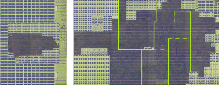
 Exynos M1 Core Layout

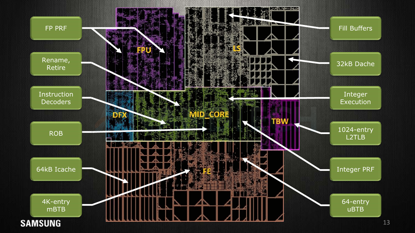
Exynos M3 Core Layout
Samsung delights us with this disclosure this year, as they break down the core’s floor plan in this slide. I’m pretty happy to have been almost accurate with the medium resolution die shot I had at hand in delimiting the various function blocks in the original review article.
Here’s some short explanations on the terms:
- pL2: Private L2 cache, here we see the 512KB cache implemented in what seems to be two banks/slices.
- FPB: Floating point data path; the FP and ASIMD execution units themselves.
- FRS: Floating point schedulers as well as the FP/vector physical register file memories.
- MC: Mid-core, the decoders and rename units.
- DFX: This is debug/test logic and stands for “design for X” such as DFD (Design for debug), DFT (Design for test), DFM (Design for manufacturability), and other miscellaneous logic.
- LS: Load/store unit along with the 64KB of L1 data cache memories.
- IXU: Integer execution unit; contains the execution units, schedulers and integer physical register file memories.
- TBW: Transparent buffer writes, includes the TLB structures.
- FE: The front-end including branch predictors, fetch units and the 64KB L1 instruction cache memories.
Exynos 9810 Floor Plan. Image Credit TechInsights
Overall compared to the M1, almost all facets of the functional units in the M3 have vastly increased in size. The end product ends up at 2.52mm² for the core’s functional blocks, plus another 0.98mm² for the 512LB L2 cache and logic.
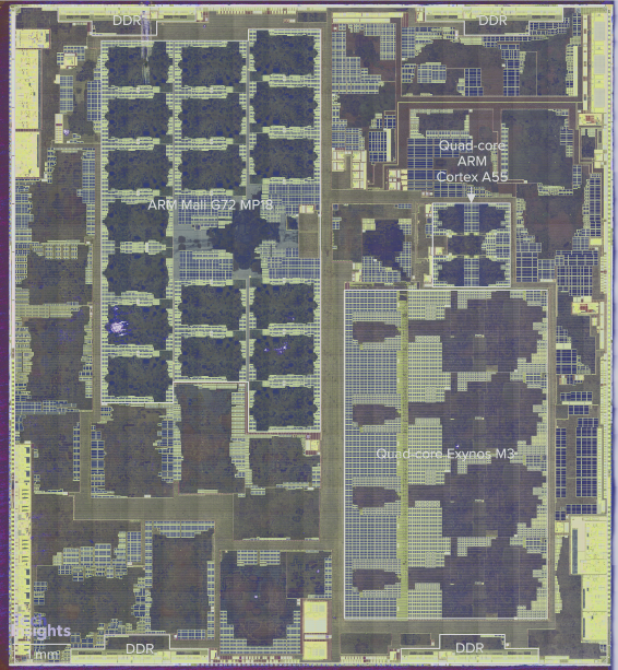
Exynos 9810 Floor Plan. Image Credit TechInsights
Here Samsung showcases the whole cluster floorplan, again marking the 4 cores laid down next to each other in a row with the L2 and L3 slides also orderly placed next to each other. This layout seems to have saved some layout efforts as each block is designed once and then simply replicated 4 times.
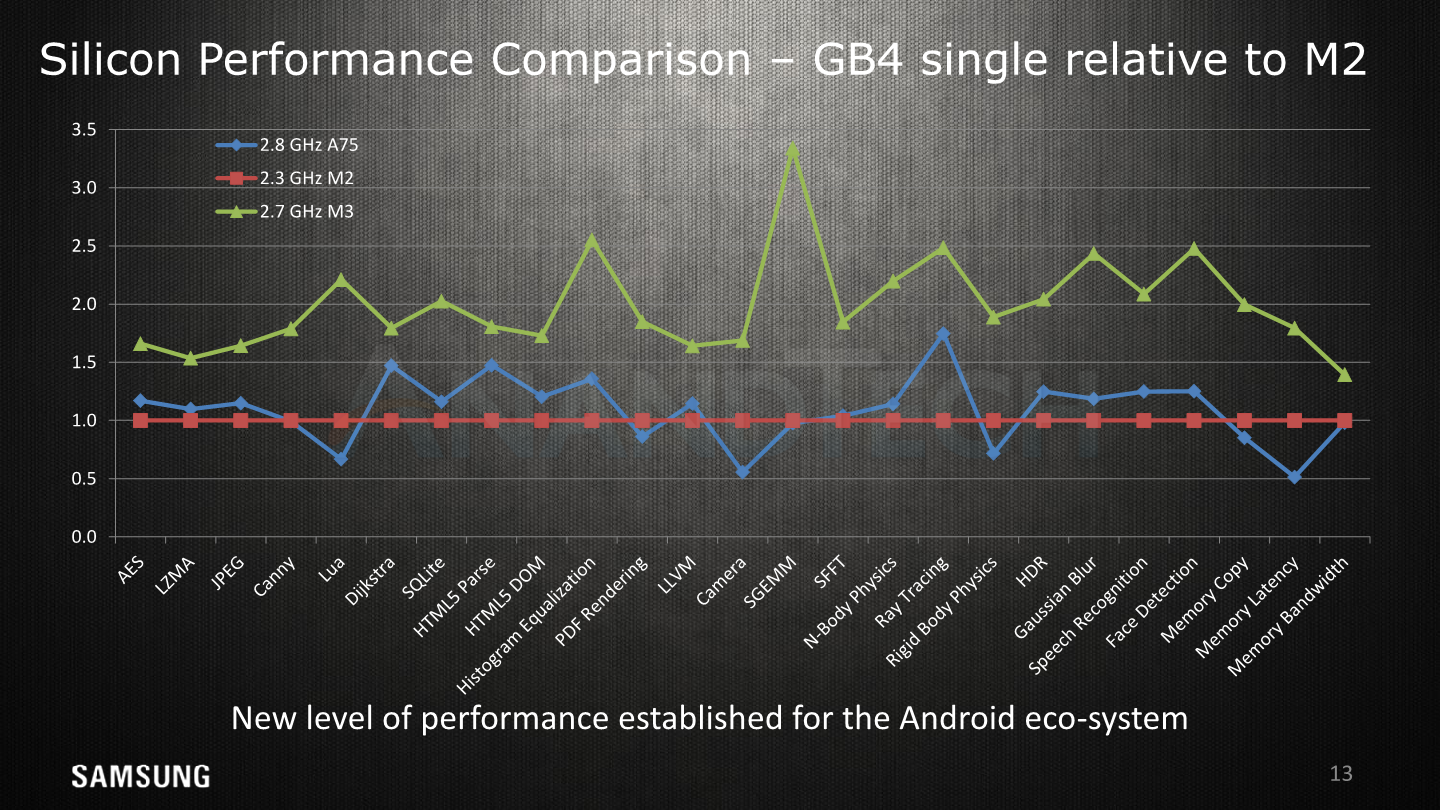
59% Higher IPC Across Variety of Workloads

Finally Samsung talks a bit about their performance profiling infrastructure and how they run various amounts of workload traces through the RTL and model simulators in order to evaluate design choices, find mistakes, and do fine-tuning to the µarch.
In this slide we finally have an official figure for the IPC increase for the core: ~59%. I had pointed out at >50% at the beginning of the year, so I'm glad to see that work out in the end. As we see in the graph, the increase is naturally not linear across all workloads and we see limited increases of only 25% in high ILP workloads, to near to not much of an increase in what is likely to be MLP workloads. Conversely, there’s also a lot of mixed workloads where the IPC increase is >80%.
Performance & Efficiency: Samsung's Data and AnandTech's Data
The next slides showcase a snippet of the performance improvements on GeekBench4 between the M2, M3, and the A75; representing commercial performance on the Exynos 8895, Exynos 9810 and the Snapdragon 845.
Again we’ve already very much extensively covered the performance aspects of the SoC and microarchitecture in past articles;
- The Samsung Galaxy S9 and S9+ Review: Exynos and Snapdragon at 960fps
- Improving The Exynos 9810 Galaxy S9: Part 1
- Improving The Exynos 9810 Galaxy S9: Part 2 - Catching Up With The Snapdragon
To add to today’s µarchitecture article I’m also adding some new SPEC scores which improve on the originally review data. The difference and cause for the improvement is DVFS tweaking, further scheduler enhancements, and a more synthetic testing environment and care with coping with the higher power draw at the M3’s maximum frequencies.

Click for large full resolution
I won’t go over the details of the scores, but the performance improvements under the new conditions more closely represents the kind of high jump Samsung showcases in GB4.
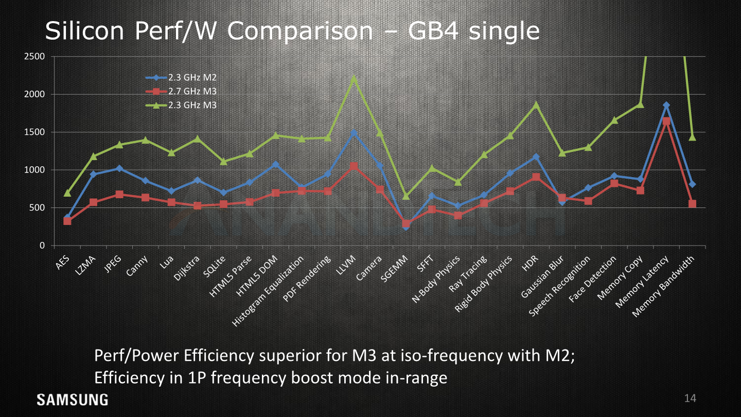
Power efficiency has been a big topic for the M3 – and here it is quite telling that they chose to omit results of competing solutions. As we’ve covered in our reviews, Samsung’s high boost clock at up to 2.7GHz comes at a price of very high required voltages and exponential power draw. Here, even though it showcases leading edge performance, it ends up less efficient than the Exynos 8895’s M2. The figures here represent active system power; that means CPU, memory controller, DRAM, much in the same way we measure it here at AT.
Reducing the clock to the same 2.3GHz as the M2, we see the M3 lead in terms of efficiency as per Samsung’s presentation.
To add to Samsung's data and give more context, I’m reposting the revised benchmark and efficiency overview in our own independently performed analysis of the platform. The below chart showcases the energy usages to finish the workload suite, alongside the average power consumption during the test. The left bars represent the consumed energy in Joures, and the shorter the bars are (the less energy), the more efficient a platform is. The right bars represent the performance score, the longer the bars denoting better performance.
I’ve also re-tested the workloads at the three top-frequencies of the M3; 1794, 2314 and 2704MHz, giving us a wider idea of how the efficiency scales with performance.

Overall the M3 offers a quite dynamic range in its results. At (almost) equivalent peak performance against the competing A75 results for this generation, the M3 is able to post a good efficiency advantage. This lower performance point of the M3 still outperforms the 2.3GHz maximum performance of the M2 – all while having significant power and energy efficiency advantages.
Clocking it up to 2.3GHz here the M3 more clearly outperforms the A75, albeit at an efficiency hit in the integer workloads, while the FP workloads closely match the Arm competition.
Finally the 2.7GHz results further the performance gap, but comes at a great cost in efficiency, using up more energy than any other recent SoC.
The fact that the E9810 had a cluster of 4 M3 cores running on the same frequency and voltage plane came at a cost of overall efficiency. Secondary threads that didn’t require the peak performance driven by a larger primary thread, but whose requirements are still bigger than the capacity of the littles cores, had to take a large the efficiency hit of running at the same bad efficiency points as the biggest thread in the cluster. The result of this adds to the bad battery life scores we’ve come to measure.
I’ve been able to resolve the scheduling issues in a custom kernel, improving the web browsing score further to 9h, however there are still compromises that just can’t be resolved due to how the SoC operates. Here I expect Samsung to depart from the 4 “huge core” topology for the next generation M4 and introduce something that will be a lot more power efficient in diverse multi-threaded scenarios.


45 Comments
View All Comments
name99 - Wednesday, August 22, 2018 - link
The issue is not technology (everyone knows CDMA basics because you need it on the data side for WCDMA aka 3G). The issue is licensing.Maybe QC changes the licensing terms so that doing it in-house was simply not worth the cost? This seems very much in-line with the world-wide lawsuits against QC for various anti-competitive behavior.
petar_b - Saturday, November 3, 2018 - link
I when they use Exynos they have less royalty fees to pay since it's their own processor. EU market is smaller than the US or ASIA so they compensate by providing chip with cheaper costs.PS - CDMA, modem and all other reasons mentioned are irrelevant; other brands use Qualcom in EU and all works perfectly.
AlB80 - Monday, August 20, 2018 - link
Unused cores do not consume energy at all regardless of voltage. Thus there should be two threads on performance cores, one requires 3 GHz, but second do not, to lose efficiency.linuxgeex - Tuesday, August 21, 2018 - link
While technically you're right that the core itself doesn't draw power when it's powered down, there's other factors to consider:1) the power cost to power it down and back up when you need it again. If you use the core intermittently then the cost of powering it up and down can exceed the cost of operating it for the workload, and then it may be more efficient to keep those jobs on the less efficient core(s)
2) the uncore, ie the busses and support logic that don't get powered down, can use nearly as much power as the cores themselves. In some CPUs, ie Ryzen2 TRW 2990WX the uncore actually consumes 76% of the die power when there's only 2 cores out of 32 active.
name99 - Monday, August 20, 2018 - link
"When Arm disclosed the A76 µarch details and particularly the 128-entry ROB (which in comparison seems quite small to the M3), they said that this was a balance between performance and area/power. In particular we saw a mention that a 7% increase in the ROB capacity only came with a 1% performance gain on average."ROB per se costs very little, it's just a queue.
What is expensive is the physical register file, and the fact that it more or less scales with the size of the ROB (since most instructions generate one value, which consumes one physical register).
The trick, then, is what can you do to increase the size of the ROB (which allows you to do more work during dead periods while your ROB-blocking instruction at the head of the queue is waiting on DRAM) without paying the cost of the register file?
There is a bag of tricks for this, and as you make your CPU more advanced, you use more and more of them. They include
- clustering (so you duplicate the register file, and have half the execution units use one of the register files, the other half use the other register file. This works because there are quadratic aspects to the register file, so cutting some things in half [even if they are then duplicated] reduces area/power by four.
- various "resource amplification" techniques getting more use out of what you have. These might be giving your register file one fewer read ports, but then having a smart allocator that can cope if the reads are oversubscribed. Or it might be delayed register allocation and early register release (so the register is held for a shorter time). Or it might be various forms of instruction fusion.
- you can try to set aside instructions that you believe will be dependent on the blocking instruction, so that they do not even get allocated a register until the blocking instruction completes. There has been some very interesting recent work on how you can do this without requiring long range communication, so while this has been talked about for 20 years, we might soon see actual implementations.
- a variant on the above is you can measure how "critical" instructions are (ie does the rest of the computation get delayed if this one instruction gets delayed. Based on this knowledge, you can send through critical instructions when resources are scarce, and delay non-critical until more resources are available.
The larger point here is that the reason Samsung et al are happy to tell you the info they are telling you (number of ROB slots, numbers of execution units, etc) is because this stuff is thoroughly uninteresting and uncompetitive. The competitive stuff is the sort of thing I have described above --- how does company A get 1.5x the performance from a certain level of HW versus company B --- and that's what no-one is ever willing to talk about...
Best you can do is see what look like good ideas in the academic literature of a few years ago and then assume that at least some of them have been picked up.
jospoortvliet - Wednesday, August 29, 2018 - link
Mja this stuff might be uninteresting for deep techies but for many it is nice to get some degree of comparison between the various CPU's being built.name99 - Monday, August 20, 2018 - link
"The fetch unit’s bandwidth has been doubled and now can read up to 48 bytes per cycle which corresponds to 12 32b instructions per cycle – this results in a 2:1 ratio of fetch versus decode capacity which is an increase over the 1.5:1 ratio (24B/c, 4 decode) in the M1. Samsung explains that the big increase is needed to combat the increasingly big problem of branch bubbles on wider microarchitectures. They admit that on average, the distance between taken branches is less than 12 instructions, but the larger width helps a lot for temporary bursts of instructions."One point you missed is that it's generally not worth the (area+power) cost to allow two lines per cycle to be read from your I-cache. So that 12-wide fetch is a maximum, which can only be reached if the starting address is one of the first four (of sixteen) instructions in the line. Every later instruction gives you a shorter fetch because you only extend to the end of the line.
Averaged across all possibilities, your average fetch width is something like nine, which is still larger than the six sustained you need, but not quite as extravagant as it seems.
It's also the case that the way these multi-level branch predictors work (at least sometimes, who knows exactly what SS are doing) is that a first fast prediction is made, then the next cycle or two, that prediction is confirmed against the larger prediction data structures. If the later prediction disagrees, you get a flush --- but ideally you can just flush what's in the I-queue before it hit decode, you don't have to flush the entire pipeline. Point is, however, you are now also using up some fraction of that 9-wide-fetch (on average) on fetches that get tossed before they even hit decode :-(
And for this to work well, you want the I-queue to ALWAYS be somewhat fullish, so you want it filling up fast, right after any sort of flush event.
So all things considered, 12-wide fetch is probably optimal, not at all extravagant.
jospoortvliet - Wednesday, August 29, 2018 - link
Keep commenting I love this ;-)eastcoast_pete - Monday, August 20, 2018 - link
Andrei, Thanks for the in-depth coverage, especially the added information from your own deep dive from a little while ago! I wonder if Samsung even commented on the software-induced self-inflicted injury that really hogtied what, by its specs, should have been a faster alternative to the A75/845. Also, did anybody from Samsung thank you for showing them how to partially improve the M3's performance in your deep dive, at least informally/in the hallway? Somehow, the M3 is a very "Samsung" product: okay - great hardware, flawed - awful software.All that being said: any mentioning or rumors on "Windows on Exynos"?
Andrei Frumusanu - Monday, August 20, 2018 - link
Today's disclosures are just on the µarch - the CPU design teams are not in charge of any of the software which is S.LSI's and Samsung Mobile's responsibilities.