The AnandTech Coffee Lake Review: Initial Numbers on the Core i7-8700K and Core i5-8400
by Ian Cutress on October 5, 2017 9:00 AM EST- Posted in
- CPUs
- Intel
- Core i5
- Core i7
- Core i3
- 14nm
- Coffee Lake
- 14++
- Hex-Core
- Hyperthreading
Silicon and Process Nodes: 14++
Despite being somewhat reserved in our pre-briefing, and initially blanket labeling the process node for these chips as ‘14nm’, we can confirm that Intel’s newest ‘14++’ manufacturing process is being used for these 8th Generation processors. This becomes Intel’s third crack at a 14nm process, following on from Broadwell though Skylake (14), Kaby Lake (14+), and now Coffee Lake (14++).
With the 8th Generation of processors, Intel is moving away from having the generation correlate to both the process node and microarchitecture. As Intel’s plans to shrink its process nodes have become elongated, Intel has decided that it will use multiple process nodes and microarchitectures across a single generation of products to ensure that every update cycle has a process node and microarchitecture that Intel feels best suits that market. A lot of this is down to product maturity, yields, and progress on the manufacturing side.
| Intel's Core Architecture Cadence (8/20) | |||||
| Core Generation | Microarchitecture | Process Node | Release Year | ||
| 2nd | Sandy Bridge | 32nm | 2011 | ||
| 3rd | Ivy Bridge | 22nm | 2012 | ||
| 4th | Haswell | 22nm | 2013 | ||
| 5th | Broadwell | 14nm | 2014 | ||
| 6th | Skylake | 14nm | 2015 | ||
| 7th | Kaby Lake | 14nm+ | 2016 | ||
| 8th | Kaby Lake Refresh Coffee Lake Cannon Lake |
14nm+ 14nm++ 10nm |
2017 2017 2018? |
||
| 9th | Ice Lake? ... |
10nm+ | 2018? | ||
| Unknown | Cascade Lake (Server) | ? | ? | ||
Kaby Lake was advertised as using a 14+ node with slightly relaxed manufacturing parameters and a new FinFET profile. This was to allow for higher frequencies and better overclocking, although nothing was fundamentally changed in the core manufacturing parameters. With Coffee Lake at least, the minimum gate pitch has increased from 70nm for 84nm, with all other features being equal.
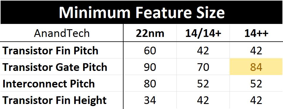
Increased gate pitch moves transistors further apart, forcing a lower current density. This allows for higher leakage transistors, meaning higher peak power and higher frequency at the expense of die area and idle power.
Normally Intel aims to improve their process every generation, however this seems like a step ‘back’ in some of the metrics in order to gain performance. The truth of the matter is that back in 2015, we were expecting Intel to be selling 10nm processors en-masse by now. As delays have crept into that timeline, the 14++ note is holding over until 10nm is on track. Intel has already stated that 10+ is likely to be the first node on the desktop, which given the track record on 14+ and 14++ might be a relaxed version of 10 in order to hit performance/power/yield targets, with some minor updates. Conceptually, Intel seems to be drifting towards seperate low-power and high-performance process nodes, with the former coming first.
Of course, changing the fin pitch is expected to increase the die area. With thanks to HEKPC (via Videocardz), we can already see a six-core i7-8700K silicon die compared to a quad-core i7-7700K.
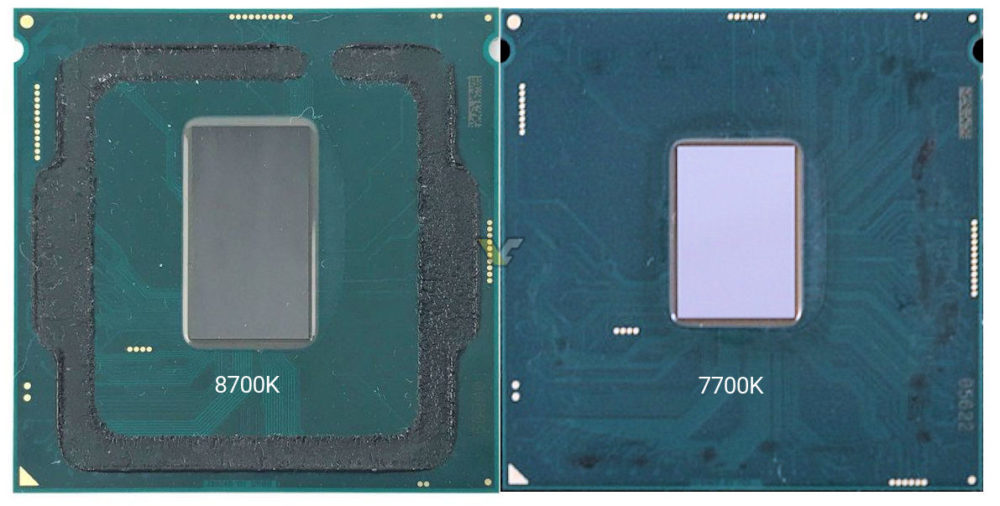
The die area of the Coffee Lake 6+2 design (six cores and GT2 graphics) sits at ~151 mm2, compared to the ~125 mm2 for Kaby Lake 4+2 processor: a 26mm2 increase. This increase is mainly due to the two cores, however there is a minor adjustment in the integrated grpahics as well to support HDCP 2.2, not to mention any unpublished changes Intel has made to their designs between Kaby Lake and Coffee Lake.
The following calculations are built on assumptions and contain a margin of error
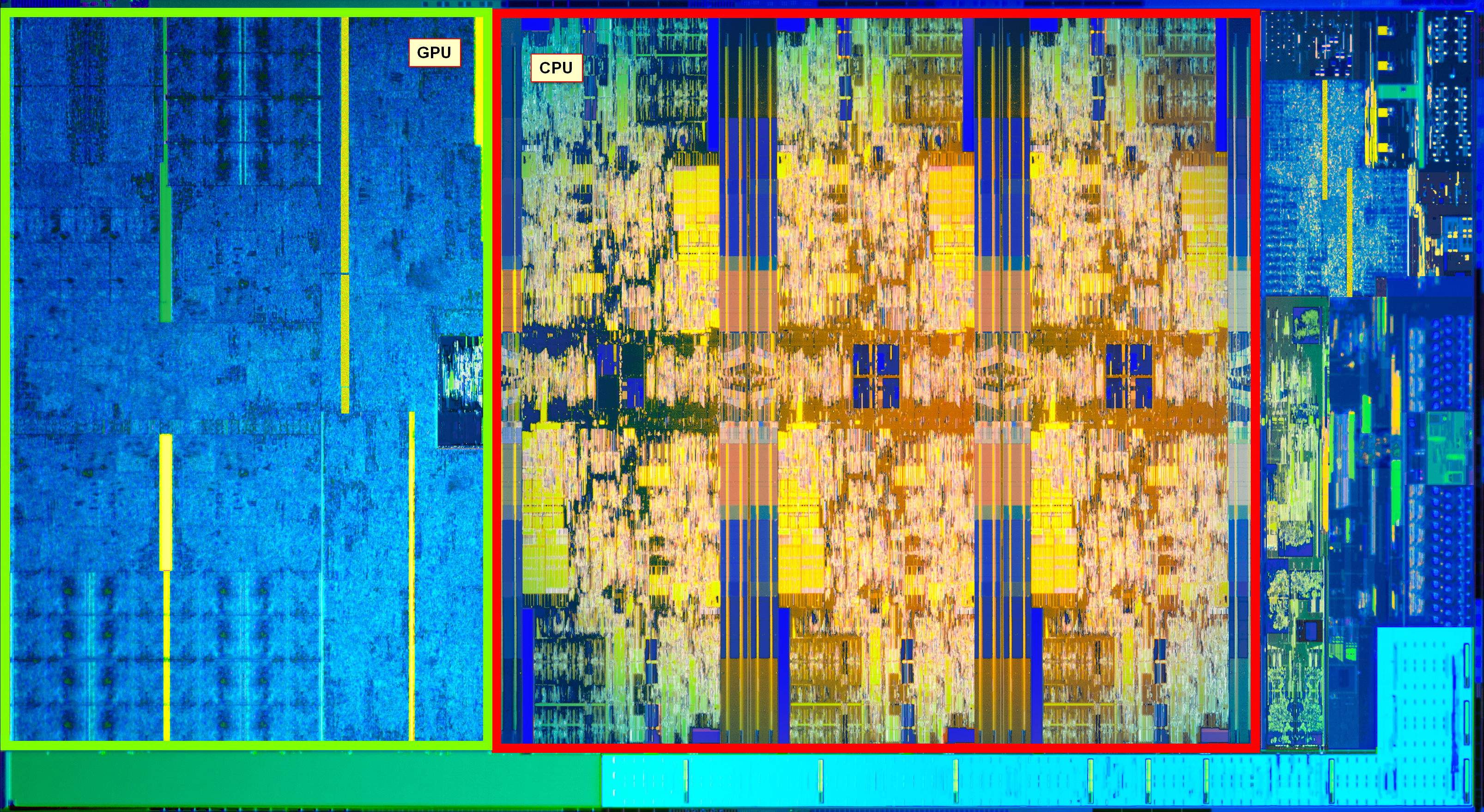
With the silicon floor plan, we can calculate that the CPU cores (plus cache) account for 47.3% of the die, or 71.35 mm2. Divided by six gives a value of 11.9 mm2 per core, which means that it takes 23.8 mm2 of die area for two cores. Out of the 26mm2 increase then, 91.5% of it is for the CPU area, and the rest is likely accounting for the change in the gate pitch across the whole processor.
The Coffee Lake 4+2 die would then be expected to be around ~127 mm2, making a 2mm2 increase over the equivalent Kaby Lake 4+2, although this is well within the margin of error for measuring these processors. We are expecting to see some overclockers delid the quad-core processors soon after launch.
In previous Intel silicon designs, when Intel was ramping up its integrated graphics, we were surpassing 50% of the die area being dedicated to graphics. In this 6+2 design, the GPU area accounts for only 30.2% of the floor plan as provided, which is 45.6 mm2 of the full die.
Memory Support on Coffee Lake
With a new processor generation comes an update to memory support. There is always a small amount of confusion here about what Intel calls ‘official memory support’ and what the processors can actually run. Intel’s official memory support is typically a guarantee, saying that in all circumstances, with all processors, this memory speed should work. However motherboard manufacturers might offer speeds over 50% higher in their specification sheets, which Intel technically counts as an overclock.
This is usually seen as Intel processors having a lot of headroom to be conservative, avoid RMAs, and maintain stability. In most cases this is usually a good thing: there are only a few niche scenarios where super high-speed memory can equate to tangible performance gains* but they do exist.
*Based on previous experience, but pending a memory scaling review
For our testing at least, our philosophy is that we test at the CPU manufacturers’ recommended setting. If there is a performance gain to be had from slightly faster memory, then it pays dividends to set that as the limit for official memory support. This way, there is no argument on what the rated performance of the processor is.
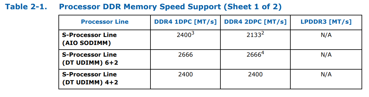
For the new generation, Intel is supporting DDR4-2666 for the six-core parts and DDR4-2400 for the quad-core parts, in both 1DPC (one DIMM per channel) and 2DPC modes. This should make it relatively simple, compared to AMD’s memory support differing on DPC and type of memory.
It gets simple until we talk about AIO designs using the processors, which typically require SODIMM memory. For these parts, for both quad-core and hex-core, Intel is supporting DDR4-2400 at 1DPC and DDR4-2133 at 2DPC. LPDDR3 support is dropped entirely. The reason for supporting a reduced memory frequency in an AIO environment with SODIMMs is because these motherboards typically run their traces as chained between the memory slots, rather than a T-Topology which helps with timing synchronization. Intel has made the T-Topology part of the specification for desktop motherboards, but not for AIO or integrated ones, which explains the difference in DRAM speed support.
These supported frequencies follow JEDEC official sub-timings. Familiar system builders will be used to DDR4-2133 at a CAS Latency of 15, but as we increase the speed of the modules, the latency increases to compensate:
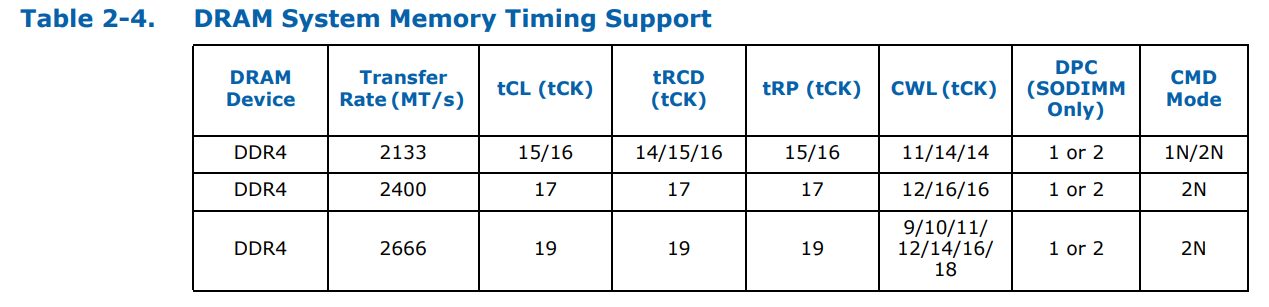
Intel’s official sub-timing support at DDR4-2666 is 19-19-19. Outside of enterprise modules, that memory does not really exist, because memory manufacturers can seem to mint DDR4-2666 16-17-17 modules fairly easily, and these processors are typically fine with those sub-timings. CPU manufacturers typically only state ‘supported frequency at JEDEC sub-timings’ and do not go into sub-timing discussions, because most users care more about the memory frequency. If time permits, it would be interesting to see just how much of a performance deficit the official JEDEC sub-timings provide compared to what memory is actually on sale.


222 Comments
View All Comments
DigitalFreak - Thursday, October 5, 2017 - link
Anyone having an issue with Bench? I'm trying to compare my i7-3770k to the i7-8700k and it comes back with no data. Same with trying the Threadripper 1920xmkaibear - Friday, October 6, 2017 - link
CPU tests changed so benchmarks weren't comparable. Latest processor tested on the old tests was the 7700K iirc, and not everything is tested on the new tests.I'd compare results for the 3770k and the 2600K to get a baseline then you can compare 2600K to the 8700K. It's a bit fiddly, I have to do the same with my 4790K.
Ian Cutress - Saturday, October 7, 2017 - link
We updated our CPU testing suite for Windows 10 in Q1. Regression testing is an on-going process, though it's been slow because of all the CPU launches this year. Normally we have 1/2 a year. We're so far at what, 6 or 7 for 2017?mczak - Thursday, October 5, 2017 - link
Doesn't look to me like the die size actually increased at all due to the increased gate pitch.The calculations in the article forgot to account for the increase of the unused area (at the bottom left) - this area is tiny with 2c die, but increases with each 2 cores added significantly. By the looks of it, that unused area would have grown by about 2 mm^2 or so going from 4 to 6 cores, albeit I'm too lazy to count the pixels...
jjj - Thursday, October 5, 2017 - link
Your conclusion is weirdest thing ever, you fully ignore the 8359k and AMD.In retail, the 8350k will do very very well and retail is what matters for most readers
And ignoring AMD is not ok at all, it's like you think that we are all idiots that buy on brand.You do think that, your system guides make that very clear but you should not accept, support and endorse such an idiotic behavior.
AMD got hit hard here, Intel takes back the lead and it's important to state that. Sure they might have Pinnacle Ridge in a few months and take back the lead but buyers that can't wait should go with Intel right now, for the most part. AMD could also adjust prices ofc.
Tigris - Thursday, October 5, 2017 - link
Really confused why the pricing listed in this review isn't consistent- for Intel you were posting prices you found online, but for Ryzen you appear to be posting MSRP.The truth is- you can find 1700x for $298 right now EASILY (Amazon), yet Microcenter is selling the 8700k for $499.
If you factor this information in, the AMD solutions are still far more valuable per dollar.
wolfemane - Thursday, October 5, 2017 - link
I really can’t belive the amount of flak Anandtech takes these days. I find it un-earned an unwarrented. Out of all the tech sites and forums I manage to read in a given week, Anandtech is the most often quoted and linked to. Hell I use it as my go to for reference and comparison (and general reading). My only big complaint is your ads, and I’d gladly pay a sub to completely remove that nonsense and directly support the site!Ian, you and your staff deserve far more credit than you get and that’s an injustice. Each piece is pretty thorough and pretty spot on. So for that thank you very much.
This article is no exception to the rule and is superb. Your graph layouts are a welcome feature!!!!! I look forward to your ever expanding tests as new chips roll in. I think the 8600k is going to be a game changer in the i5 vs i7 performance category for these hexacore cpus. I think that’s why almost all the reviews I’m reading today are with the 8700k and 8400.
Agin, thank you and your staff very much for the work you put into publishing amazing articles!!
vanilla_gorilla - Thursday, October 5, 2017 - link
Personally I buy whatever is best at the time. Right now I'm typing this on a 1700x and I can see a 4770k build on the desk next to me. So it's always funny to see the bias. Intel review gets posted, AMD fanboys come out of the wood works to trash them as paid shills. But it works exactly the same on any positive AMD reviews. Intel fans come in trashing them. It's really odd. Anandtech is one of the most unbiased sites I've found and I trust their reviews implicitly.mkaibear - Saturday, October 7, 2017 - link
> Anandtech is one of the most unbiased sites I've found and I trust their reviews implicitly.Yep. Anyone who looks at AT and sees bias needs to examine their own eyesight.
SeannyB - Thursday, October 5, 2017 - link
For the H.264 encoding tests, you could consider using the "medium" preset or better. The "very fast" preset has a tendency to use fewer cores.