The Intel Core i9-7980XE and Core i9-7960X CPU Review Part 1: Workstation
by Ian Cutress on September 25, 2017 3:01 AM ESTOpinion: Why Counting ‘Platform’ PCIe Lanes (and using it in Marketing) Is Absurd
It’s at this point that I’d like to take a detour and discuss something I’m not particularly happy with: counting PCIe lanes.
The number of PCIe lanes on a processor, for as long as I can remember, has always been about which lanes come directly from the PCIe root, offering full bandwidth and with the lowest possible latency. In modern systems this is the processor itself, or in earlier, less integrated systems, the Northbridge. By this metric, a standard Intel mainstream processor has 16 lanes, an AMD Ryzen has 16 or 20, an Intel HEDT processor has 28 or 44 depending on the model, and an AMD Ryzen Threadripper has 60.
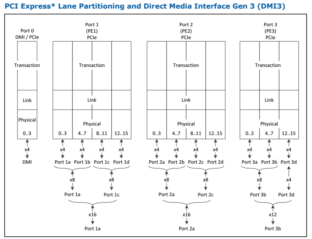
In Intel’s documentation, it explicitly lists what is available from the processor via the PCIe root complexes: here 44 lanes come from two lots of sixteen and one twelve lane complex. The DMI3 link to the chipset is in all but name a PCIe 3.0 x4 link, but is not included in this total.
The number of PCIe lanes on a chipset is a little different. Chipsets are for all practical purposes PCIe switches: using a limited bandwidth uplink, it is designed to carry traffic from low bandwidth controllers, such as SATA, Ethernet, and USB. AMD is limited in this regard, due to spending more time re-entering the pure CPU performance race over the last few years and outsource their designs to ASMedia. Intel has been increasing its PCIe 3.0 lane support on its chipsets for at least three generations, now supporting up to 24 PCIe 3.0 lanes. There are some caveats on what lanes can support which controllers, but in general we consider this 24.
Due to the shared uplink, PCIe lanes coming from the chipset (on both the AMD and Intel side) can be bottlenecked very easily, as well as being limited to PCIe 3.0 x4. The chipset introduces additional latency compared to having a controller directly attached to the processor, which is why we rarely see important hardware (GPUs, RAID controllers, FPGAs) connected to them.
The combination of the two lends itself to a variety of platform functionality and configurations. For example, for AMD's X399 platform that has 60 lanes from the processor, the following combinations are 'recommended':
| X399 Potential Configurations | |||
| Use | PCIe Lanes | Total | |
| Content Creator | 2 x Pro GPUs 2 x M.2 Cache Drives 10G Ethernet 1 x U.2 Storage 1 x M.2 OS/Apps 6 x SATA Local Backup |
x16/x16 from CPU x4 + x4 from CPU x4 from CPU x4 from CPU x4 from CPU From Chipset |
52 Lanes |
| Extreme PC | 2 x Gaming GPUs 1 x HDMI Capture Card 2 x M.2 for Games/Stream 10G Ethernet 1 x M.2 OS/Apps 6 x SATA Local Backup |
x16/x16 from CPU x8 from CPU x4 + x4 from CPU x4 from CPU x4 from CPU From Chipset |
56 Lanes |
| Streamer | 1 x Gaming GPU 1 x HDMI Capture Card 2 x M.2 Stream/Transcode 10G Ethernet 1 x U.2 Storage 1 x M.2 OS/Apps 6 x SATA Local Backup |
x16 from CPU x4 from CPU x4 + x4 from CPU x4 from CPU x4 from CPU x4 from CPU From Chipset |
40 Lanes |
| Render Farm | 4 x Vega FE Pro GPUs 2 x M.2 Cache Drives 1 x M.2 OS/Apps 6 x SATA Local Backup |
x16/x8/x8/x8 x4 + x4 from CPU x4 from CPU From Chipset |
52 Lanes |
What has started to happen is that these companies are combining both the CPU and chipset PCIe lane counts, in order to promote the biggest number. This is despite the fact that not all PCIe lanes are equal, they do not seem to care. As a result, Intel is cautiously promoting these new Skylake-X processors as having ’68 Platform PCIe lanes’, and has similar metrics in place for other upcoming hardware.
I want to nip this in the bud before it gets out of hand: this metric is misleading at best, and disingenuous at worst, especially given the history of how this metric has been provided in the past (and everyone will ignore the ‘Platform’ qualifier). Just because a number is bigger/smaller than a vendor expected does not give them the right to redefine it and mislead consumers.
To cite precedent: in the smartphone space, around 4-5 years ago, vendors were counting almost anything in the main processor as a core to provide a ‘full core count’. This meant that GPU segments became ‘cores’, special IP blocks for signal and image processing became ‘cores’, security IP blocks became ‘cores’. It was absurd to hear that a smartphone processor had fifteen cores, when the main general purpose cores were a quartet of ARM Cortex A7 designs. Users who follow the smartphone industry will notice that this nonsense stopped pretty quickly, partly due to anything being called a core, but some hints towards artificial cores potentially being placed in the system. If allowed to continue, this would have been a pointless metric.
The same thing is going to happen if the notion of ‘Platform PCIe Lanes’ is allowed to continue.


152 Comments
View All Comments
extide - Monday, September 25, 2017 - link
No, TDP should include Turbo as that is part of the base/stock operation mode of the CPU.IGTrading - Monday, September 25, 2017 - link
TDP = Total Design Power by definition.This is used to design the motherboard and the cooling system to give designers a clear limit over which the system doesn't go unless it is purposely overcloked.
Wikipedia : "The thermal design power (TDP), sometimes called thermal design point, is the maximum amount of heat generated by a computer chip or component (often the CPU or GPU) that the cooling system in a computer is designed to dissipate under any workload."
Intel : "TDP (Thermal Design Power) Intel defines TDP as follows: The upper point of the thermal profile consists of the Thermal Design
Power (TDP) and the associated Tcase value. Thermal Design Power (TDP) should be used for
processor thermal solution design targets. TDP is not the maximum power that the processor can
dissipate. TDP is measured at maximum TCASE.1"
Intel : "Due to normal manufacturing variations, the exact thermal characteristics of each individual processor are unique. Within the specified parameters of the part, some processors may operate at a slightly higher or lower voltage, some may dissipate slightly higher or lower power and some may draw slightly higher or lower current. As such, no two parts have identical power and thermal characteristics.
However the TDP specifications represent a “will not exceed” value. "
This is what we've understood by TDP in the past 21 years while in IT hardware industry.
If you have a different definition, then perhaps we're talking about different things.
whatevs - Monday, September 25, 2017 - link
Specification for 7980xe says "Thermal Design Power (TDP) represents the average power, in watts, the processor dissipates when operating at Base Frequency with all cores active under an Intel-defined, high-complexity workload. Refer to Datasheet for thermal solution requirements."There's a different specification for electrical design. This is not your ancient Xeon TDP.
IGTrading - Monday, September 25, 2017 - link
You mean the definition of TDP should change every year to suit Intel's marketing ?! :)"Ancient" Xeon TDP ?! :)
I've quoted Intel's own definition.
If the company just came up with a NEW and DIFFERENT definition just for the Core i9 series, then that's just plain deceiving marketing, changing with the wind (read : new generation of products) .
Plus, why the heck are they calling it TDP ?!
If they now claim that TDP "represents the average power, in watts, the processor dissipates when operating at Base Frequency with all cores active " then they basically use AMD's ACP from 2011.
What a load of nonsense from Intel ...
https://www.intel.com/content/dam/doc/white-paper/...
whatevs - Monday, September 25, 2017 - link
You have quoted 6 year old Xeon definition, different products have different operating conditions, deal with it.Spunjji - Monday, September 25, 2017 - link
Your name suggests that you're kind of a dick and your comments confirm it. Your point is weak and doesn't at all do the work you think it does.whatevs - Monday, September 25, 2017 - link
You may be unhappy with what Intel promised you, but to claim that you could burn a system with increased power usage from turbo clocks is ridiculous, thermal throttling is not fire, and it's ridiculous to argue on a cpu that can run overclocked at >400w power consumption.Notmyusualid - Monday, September 25, 2017 - link
+1wolfemane - Tuesday, September 26, 2017 - link
You can't talk rationale with a loyalist sympathizer. TDP is a set definition in the industry and one Intel seems to be misleading about with their Extreme HEDT CPU. That seems to be a fact clearly made among almost all reviews of the 7980xe.I think I read a few articles yesterday talking about how the 7980xe was having major issues and wasn't boosting correctly but showing high power draw. But yesterday was a long time ago and I cant remember where I read that.
someonesomewherelse - Saturday, October 14, 2017 - link
So why not call it 'Average Design Power - ADP'?