Analyzing Falkor’s Microarchitecture: A Deep Dive into Qualcomm’s Centriq 2400 for Windows Server and Linux
by Ian Cutress on August 20, 2017 11:00 AM EST- Posted in
- CPUs
- Qualcomm
- Enterprise
- SoCs
- Enterprise CPUs
- ARMv8
- Centriq
- Centriq 2400
Getting Intimate with Falkor: The Front End
So we have to admit that we were surprised by Qualcomm releasing so much information about the pipeline. When we’ve ever asked the mobile CPU team about Krait and Kryo, we usually hit a brick wall, left with a PR answer of a ‘custom core design’ or the guide of ‘protecting our design’. So when Falkor was offered on a plate, we grabbed a knife and a chopstick to devour the soup at hand.
The headline features are as follows:
- Variable length pipelines, 10-15 stage depending on instruction
- 4-wide decode (3 + 1 branch)
- 8-wide out-of-order dispatch
- 8 execution ports
- Micro-op cache / L0 I-cache with Way prediction
- Retire 4/cycle usually (some situations >4)
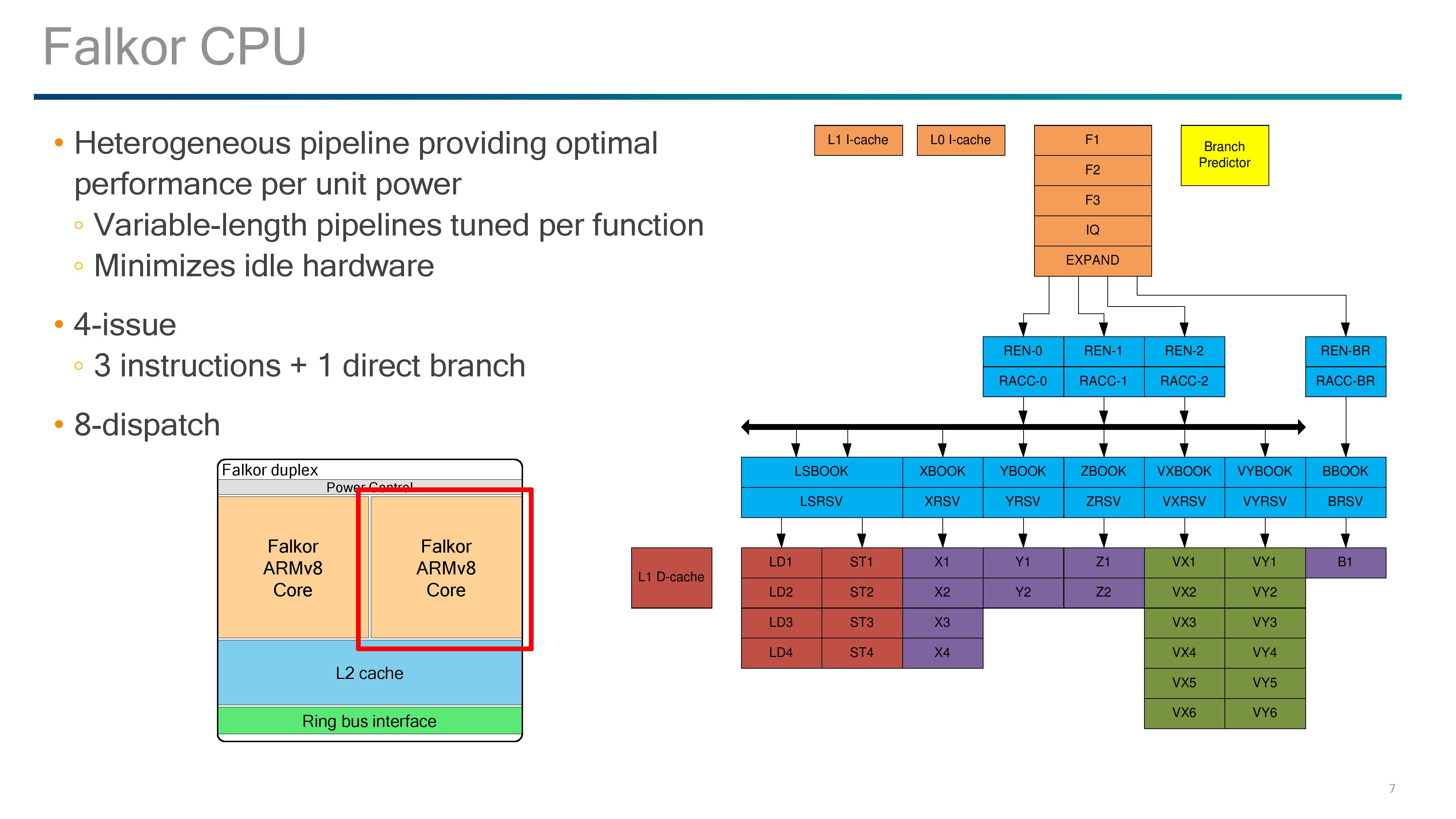
Much like most modern cores and those built on ARM’s instruction sets, pipeline lengths vary for the different execution ports, and Qualcomm states that these are tuned depending on the instruction at play.
Just to add some terminology changes in here: what Intel calls a scheduler, ARM calls an Issue Queue, and Qualcomm calls a ‘Reserve’.
We start with a 4-stage instruction fetch, with the design able to fetch up to four instructions per cycle. These go into a single stage decode that converts the instructions into micro-ops, with most instructions becoming a single micro-op. Branches out of the decode are fed into their own branch rename stage and issue queue, before hitting its own execution port. Micro-ops not fed into the branch stage go into the single-stage rename and single-stage ‘register acccess’ followed by the out-of-order dispatch window.
Up to eight instructions can move into the two-stage Reserves/issue queues, with each execution port having one Reserve except for the load/store units which have a combined Reserve. Loads and stores take 4 stages, ALUs take 2 stages (most) or 4 stages (MUL), while FP and vector pipes take six stages.
For the fetch stages of the pipeline, Qualcomm doesn’t say much about its prefetch policies here. However we do have information about the branch predictor and L0/L1 caches.
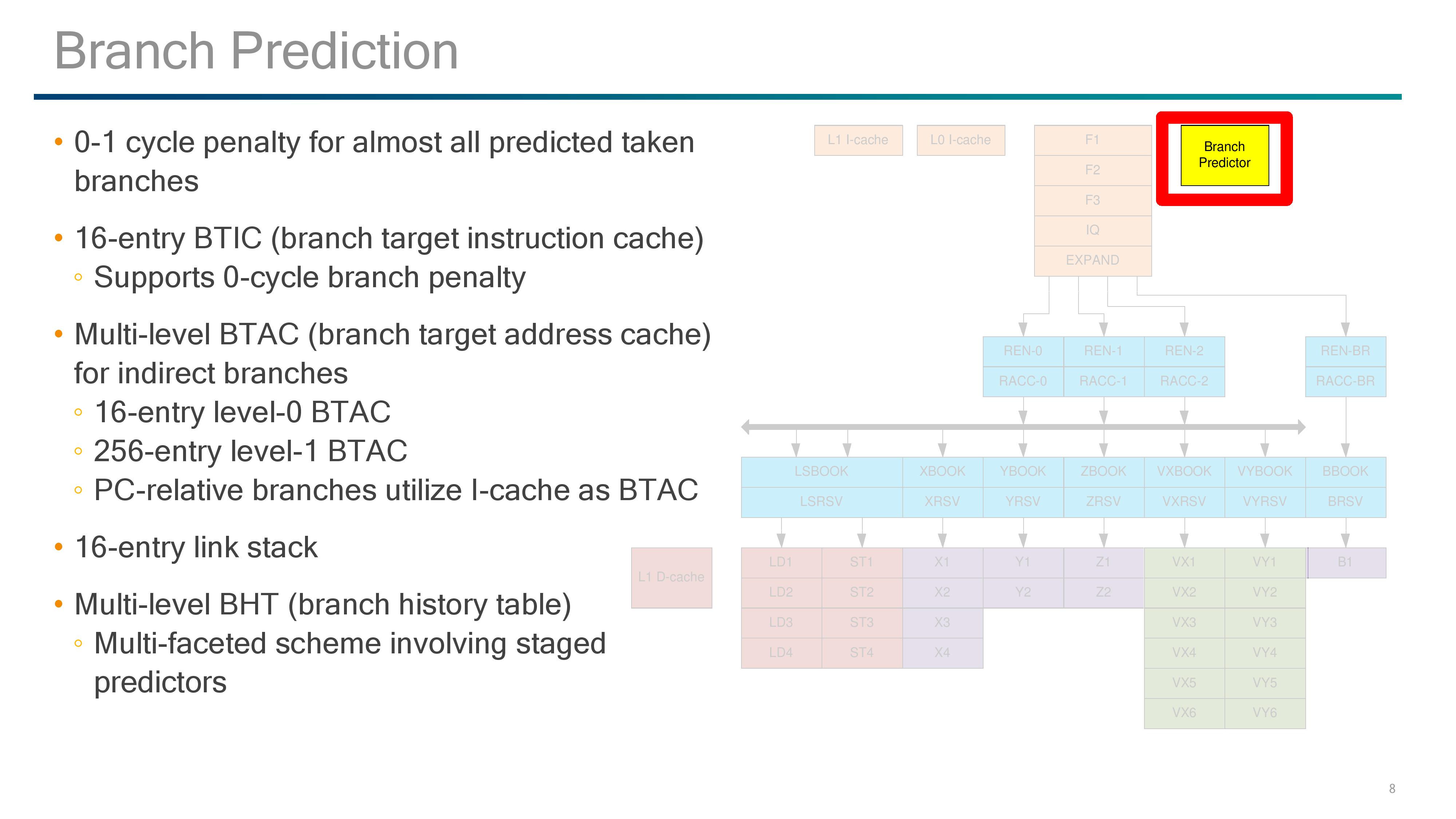
The Front End: Prefetch and Branch Predictor
Qualcomm has implemented a custom branch predictor, and the design gives a 0-1 cycle latency penalty for taking most predicted branches. For instructions, there is a 16-entry branch target instruction cache (BTIC) that supports 0-cycle access, and for addresses there is a two-level branch target address cache (BTAC) for indirect branches: a 16-entry level 0 and a 256-entry level 1. This combines with the 16-entry link stack and multi-level branch history table for predictions.
The Front End: L0/L1 Instruction Caches
The instruction caches are an interesting part of the design, with Qualcomm implementing an L0 I-cache and an L1 I-cache. Qualcomm has implemented L0 caches before, since Krait, but when I initially saw it in this design I instantly thought it looks like a micro-op cache. (in LLVM commits it even states it as a micro-op cache). Normally the test is that if it walks like a micro-op cache and talks like a micro-op cache then it’s a micro-op cache, but the difference here is that rather than storing already-decoded micro-ops, it stores instructions ready to decode.
The special element to the L0 instruction cache here is that it is Way-predicted, meaning that the cache is checked for the instruction as the prefetch also checks the L1. As the L0 is smaller and closer to the event, it offers a 0-cycle latency for any instruction that achieves an L1 hit. The L0 sits at 24 KB, using 64-byte lines and 3-way associativity, but due to the way prediction, the L0 itself is transparent to software and will be seen as part of the L1 cache when metrics probe the size and capability.
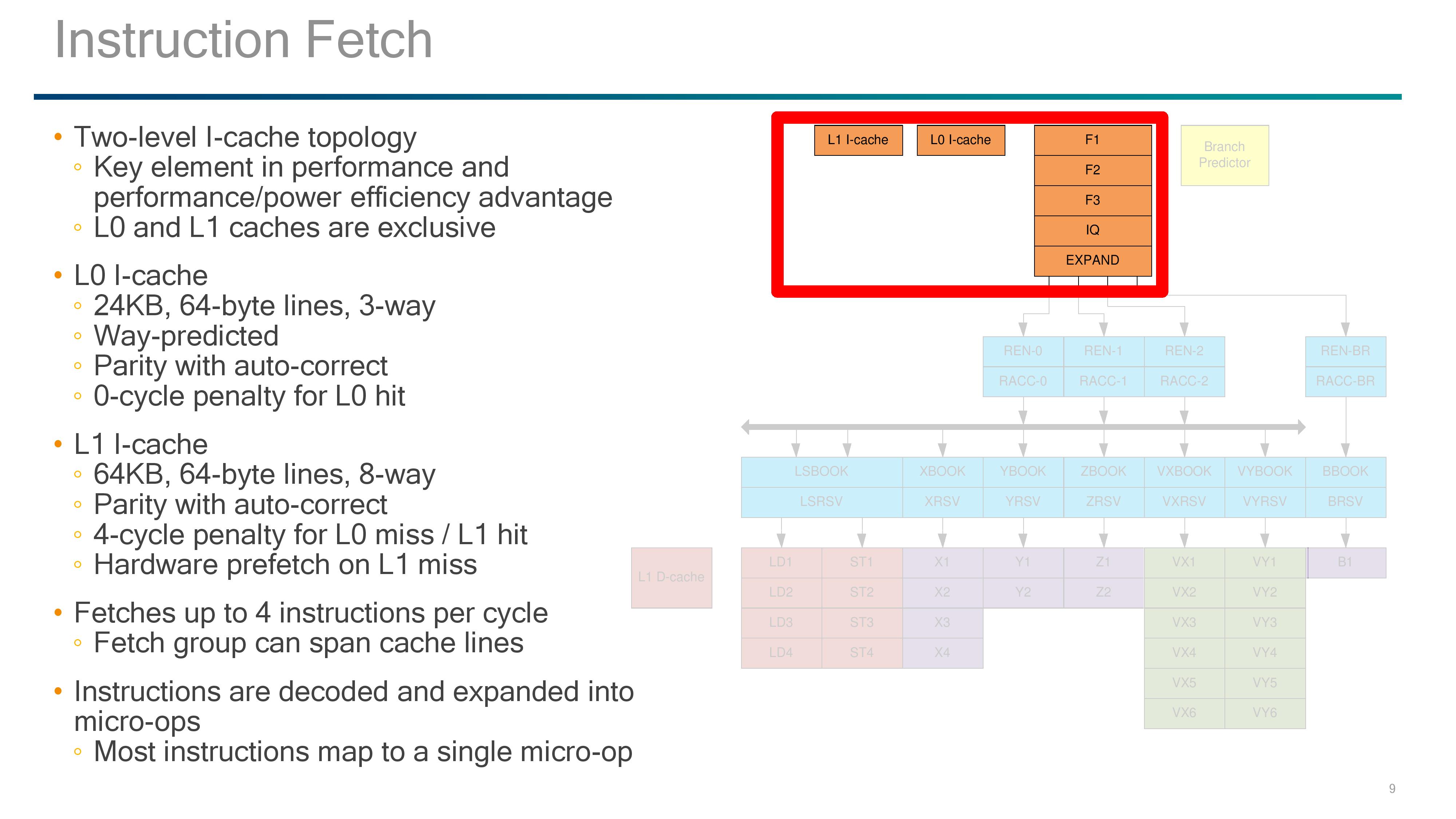
The L1 I-cache is 64KB, which is similar to other ARM architecture core designs, and also uses 64-byte lines but with an 8-way associativity. To software, as the L0 is transparent, the L1 I-cache will show as an 88KB cache. Both the L0 and L1 have parity with auto-correct, and the L1-I has a four cycle penalty on an L0 miss. An L1 miss will initiate a hardware prefetch.
Instructions that go through the fetch end up in the decoders, with the Falkor design supporting 4-issue decode (3 decode + one branch).
The Front End: Rename, Register Access and Reserve (Rename and Dispatch)
It’s worth noting at this point that Qualcomm’s slides seem to make instructions and micro-ops interchangeable at this point, or rather use the term ‘instruction’ where they mean ‘micro-op’.
Direct branches out of the decoder hit their own rename and dispatch pipeline and execution, so the main focus is on the three other decoded micro-ops. Each of these hits the rename and completion buffer, which can support up to 256-entries.
The Qualcomm diagram gets a bit odd here as after the rename/register access stages, the micro-ops hit the out-of-order dispatch buffer. This supports 76 committed micro-ops ready for dispatch or retirement while 128 uncommitted micro-ops can remain in flight, although Qualcomm doesn’t state if these numbers include the Direct Branch decode (it’s worth noting that A73/A75 do not, but A53 does).
The dispatch buffer can push through eight micro-ops per cycle into the reserve stations/issue queues, although only one reserve will serve each execution port, much like a Cortex-A75 design. This means that in order to dispatch eight per cycle, it needs one of each of the execution ports in play. The exceptions to the rule are the two load/store units that use a combined reserve station.


41 Comments
View All Comments
dennisAustin - Thursday, August 31, 2017 - link
Interesting...when I first read about it nearly a half-decade ago - even Intel and AMD have shorter design cycles _and_ x86 architecture is orders of magnitude more complex than ARM's. The target market for "Lunesta" or "Centriq?" is the data center, not angry birds, Spec, or HPC. ARMs RAS specification is in its infancy at best and likely scantly implemented in Lunesta.It was a great concept - but the window of opportunity has long sense passed - 5ish years in and likely $1B+ invested, it's a non starter. My advice - drop the IBM managers, re-hire managers with technical backgrounds -- remember this product is being driven by the same guy who said "who needs 64 bits?" -- unfortunate