Analyzing Falkor’s Microarchitecture: A Deep Dive into Qualcomm’s Centriq 2400 for Windows Server and Linux
by Ian Cutress on August 20, 2017 11:00 AM EST- Posted in
- CPUs
- Qualcomm
- Enterprise
- SoCs
- Enterprise CPUs
- ARMv8
- Centriq
- Centriq 2400
The Duplex and Power Management
Like many processors on the market, design companies will use building blocks to assemble their complete processors. Equip those blocks with the right protocols, put them together, optimize, and create an advanced piece of sand that can decompress cat gifs if we prod it in the right way. Qualcomm’s main building block at the SoC level is the Falkor duplex, containing two Falkor cores, a shared L2 cache, QSB/fabric connectivity, and represents the lowest level of power management.
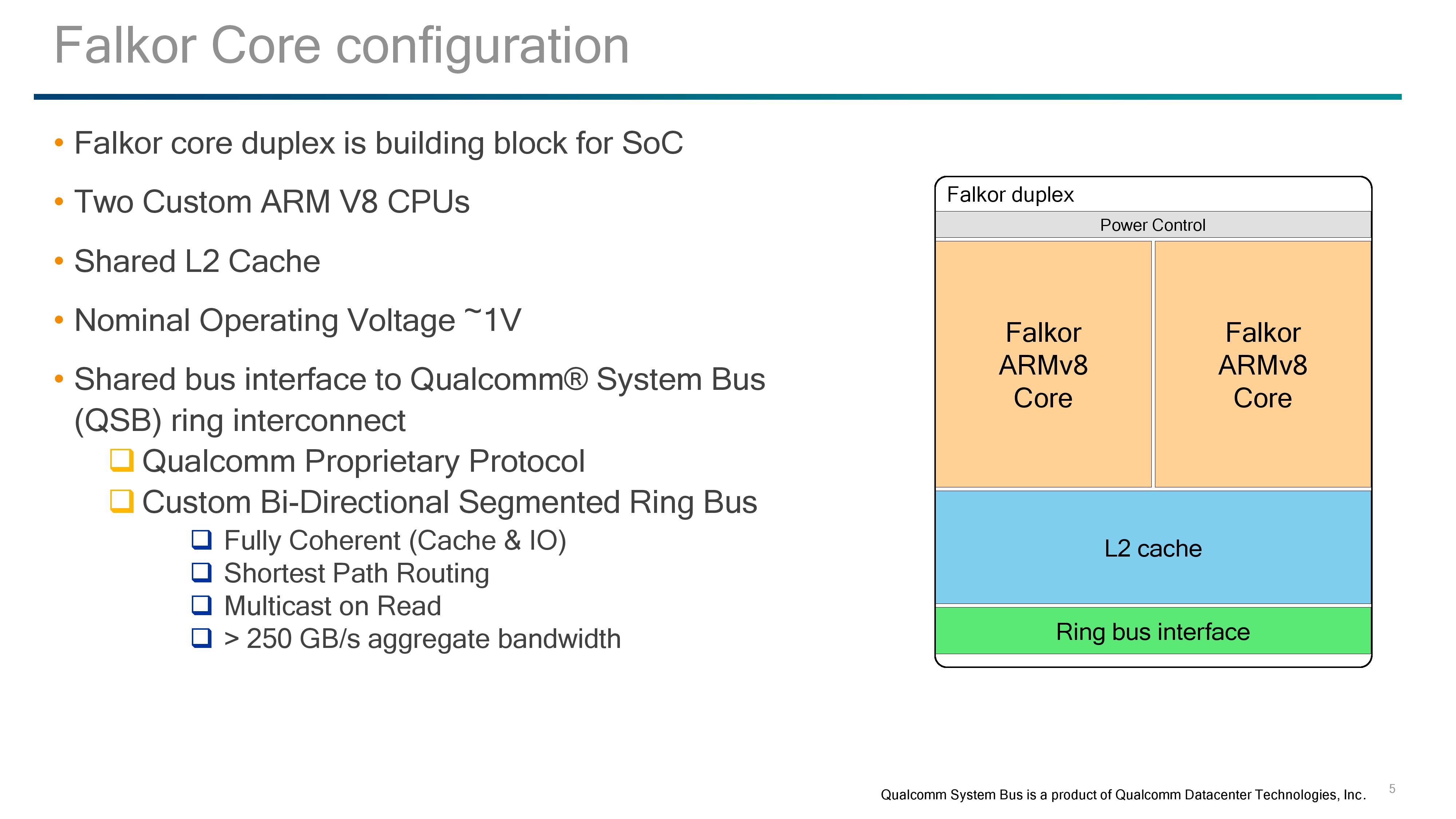
For SoC design followers, one might look at this design and think they see similarities with other dual-core designs such as AMD’s original Bulldozer design from 2011 or Intel's Xeon Phi. Internally, the cores are completely separate in terms of instruction throughput with no shared resources before the L2 cache. Consequently, between the two ends of the spectrum, Falkor is much closer to a Xeon Phi dual-core module, where each core has its own set of execution ports and vector extensions, but share an L2 cache and network connectivity.
But before diving into the cores, the L2 cache and power control require some explaining.
The L2 cache is a unified cache between both cores with ECC support, and inclusive of the L1-Data caches on both. Accesses are 128-byte interleaved with 128-byte lines, with 32-bytes per direction per interleave per cycle and 8-way associativity. ECC is using SEC-DED methodology, and the overall result as a minimum 15 cycle latency for an L2 hit, which is very competitive in the market. Qualcomm isn’t stating the size of the L2 cache at this time, which is somewhat of a surprise. In the market we see a variety of L2 cache options, so Qualcomm might end up offering a series of processors with different amounts of L2, especially if L2 defects are a factor in the manufacturing.

For power control, Qualcomm uses this unified design to control both cores. During our briefing we were told that both cores have to share the same frequency for L2 consistency; however the voltage per core can be adjusted and optimized for the best power implementation. As a result, power states between the cores can vary, and depending on the workflow needed, the cores and the L2 can also have different power states.
The cores in the duplex are powered by a block head switch or a low-dropout regulator (LDO), depending on the requirement. This allows for a variety of power down modes for the core logic, registers and caches:
- Light Sleep: CPU Clock is gated/lowered
- Voltage Retention: Registers and Caches retain state, logic is effectively off
- Register Retention: Registers retail state using main chip power rail, caches are off
- Collapse: Registers and L1 state not retained
The power control also maintains the state of the L2 cache, which offers modes similar to the CPU and may clock gate completely even with the CPUs in use. We confirmed that the L2 cache can only be on or off, and not in a half-use state.
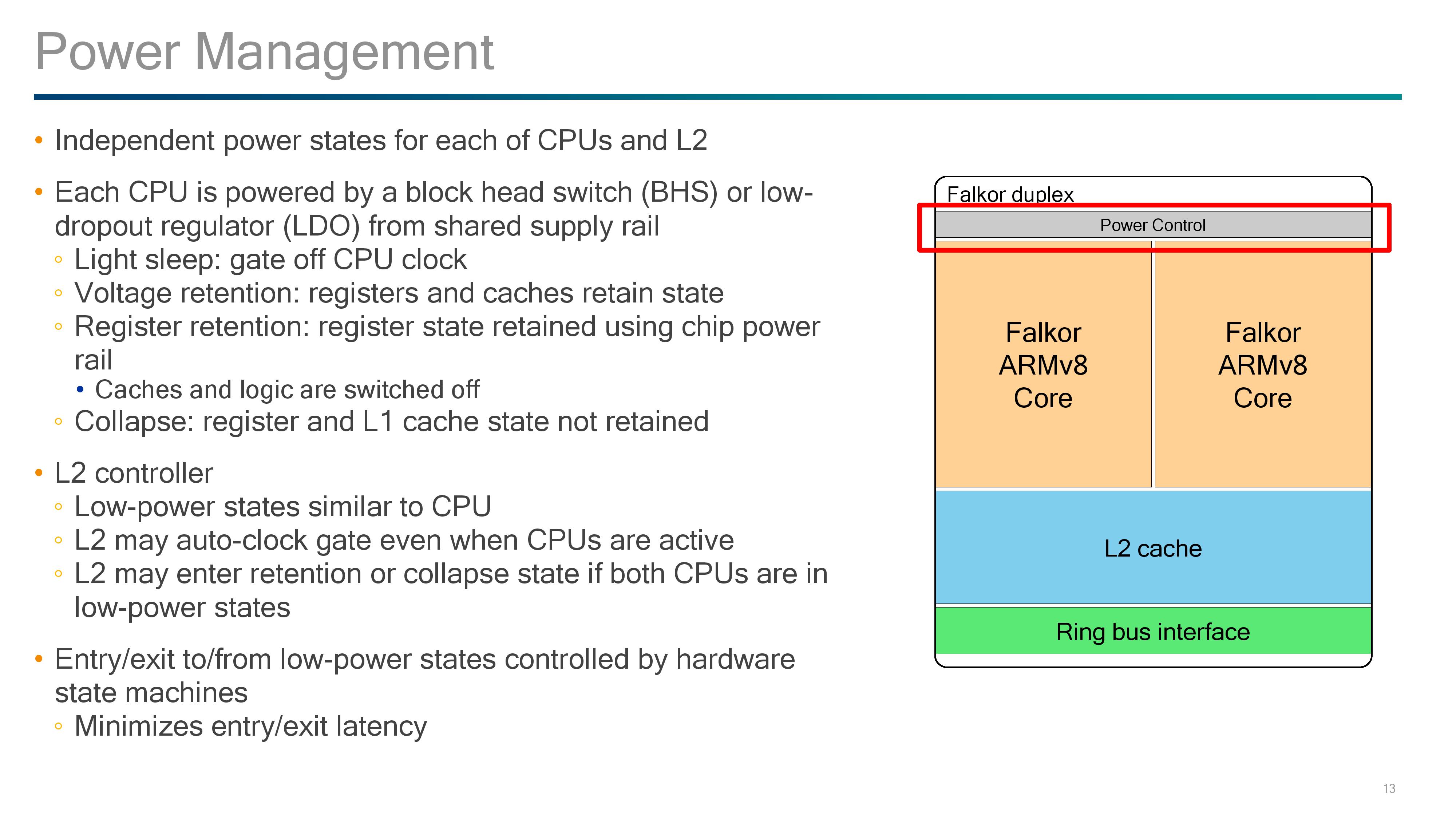
Overall for power, Qualcomm is also implementing hardware state machines, to enable quick entry and exit to and from low power modes. Qualcomm explained that CPU use in data centers can be super low depending on time of day and requirements, so the ability to save power wake quickly was a fundamental design aspect for this chip, with the aim of reducing the electricity bill.
We know that these chips are built on a 10nm process, and when questioned Qualcomm stated that they will run above 2.0 GHz, while talking in about 1.0 V to do so while also being competitive in performance per watt. Unfortunately requests regarding TDP were returned with 'competitive for a data center environment'.


41 Comments
View All Comments
dennisAustin - Thursday, August 31, 2017 - link
Interesting...when I first read about it nearly a half-decade ago - even Intel and AMD have shorter design cycles _and_ x86 architecture is orders of magnitude more complex than ARM's. The target market for "Lunesta" or "Centriq?" is the data center, not angry birds, Spec, or HPC. ARMs RAS specification is in its infancy at best and likely scantly implemented in Lunesta.It was a great concept - but the window of opportunity has long sense passed - 5ish years in and likely $1B+ invested, it's a non starter. My advice - drop the IBM managers, re-hire managers with technical backgrounds -- remember this product is being driven by the same guy who said "who needs 64 bits?" -- unfortunate