Analyzing Falkor’s Microarchitecture: A Deep Dive into Qualcomm’s Centriq 2400 for Windows Server and Linux
by Ian Cutress on August 20, 2017 11:00 AM EST- Posted in
- CPUs
- Qualcomm
- Enterprise
- SoCs
- Enterprise CPUs
- ARMv8
- Centriq
- Centriq 2400
Getting Intimate with Falkor: The Front End
So we have to admit that we were surprised by Qualcomm releasing so much information about the pipeline. When we’ve ever asked the mobile CPU team about Krait and Kryo, we usually hit a brick wall, left with a PR answer of a ‘custom core design’ or the guide of ‘protecting our design’. So when Falkor was offered on a plate, we grabbed a knife and a chopstick to devour the soup at hand.
The headline features are as follows:
- Variable length pipelines, 10-15 stage depending on instruction
- 4-wide decode (3 + 1 branch)
- 8-wide out-of-order dispatch
- 8 execution ports
- Micro-op cache / L0 I-cache with Way prediction
- Retire 4/cycle usually (some situations >4)
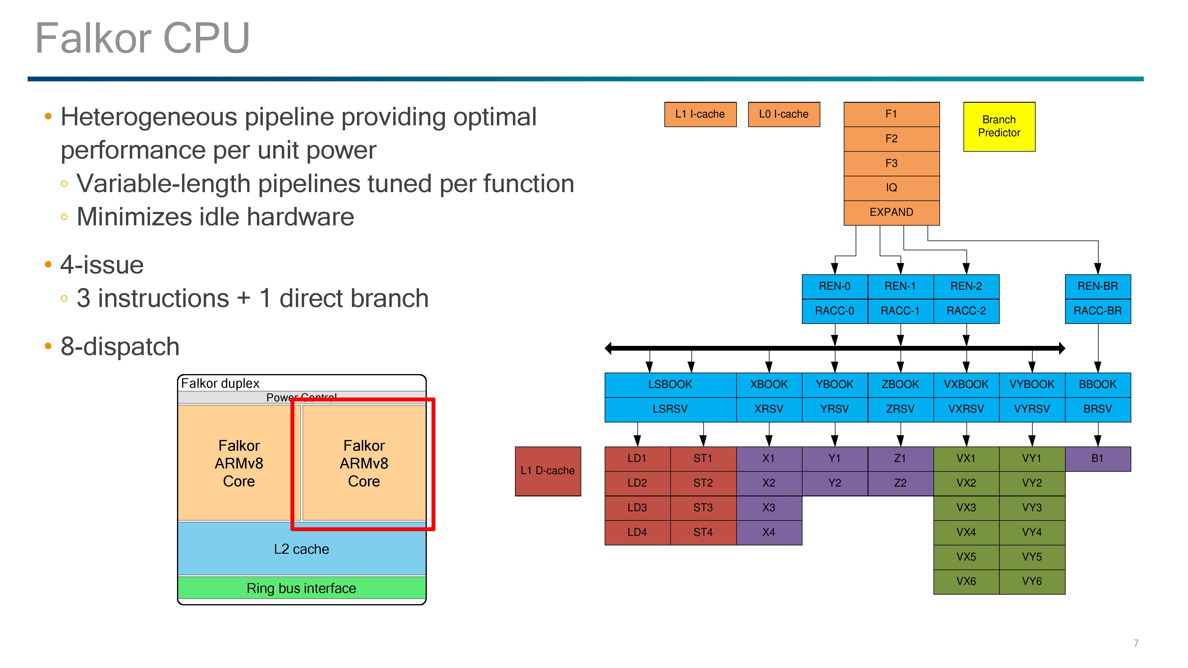
Much like most modern cores and those built on ARM’s instruction sets, pipeline lengths vary for the different execution ports, and Qualcomm states that these are tuned depending on the instruction at play.
Just to add some terminology changes in here: what Intel calls a scheduler, ARM calls an Issue Queue, and Qualcomm calls a ‘Reserve’.
We start with a 4-stage instruction fetch, with the design able to fetch up to four instructions per cycle. These go into a single stage decode that converts the instructions into micro-ops, with most instructions becoming a single micro-op. Branches out of the decode are fed into their own branch rename stage and issue queue, before hitting its own execution port. Micro-ops not fed into the branch stage go into the single-stage rename and single-stage ‘register acccess’ followed by the out-of-order dispatch window.
Up to eight instructions can move into the two-stage Reserves/issue queues, with each execution port having one Reserve except for the load/store units which have a combined Reserve. Loads and stores take 4 stages, ALUs take 2 stages (most) or 4 stages (MUL), while FP and vector pipes take six stages.
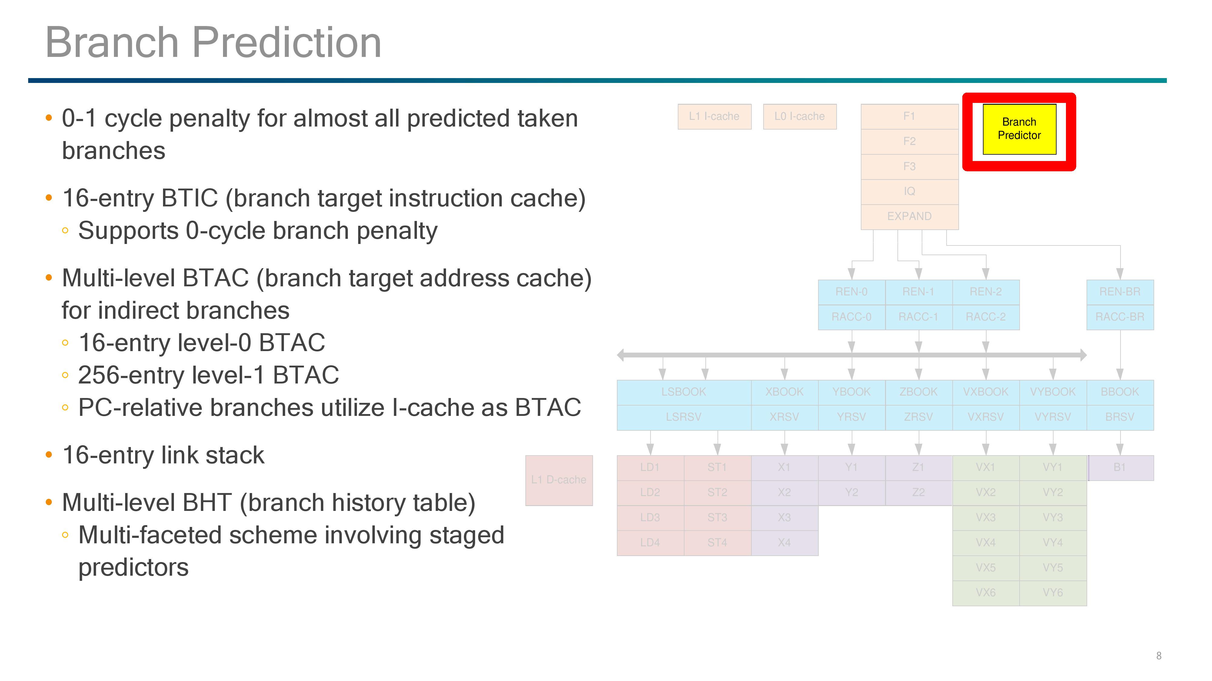
For the fetch stages of the pipeline, Qualcomm doesn’t say much about its prefetch policies here. However we do have information about the branch predictor and L0/L1 caches.
The Front End: Prefetch and Branch Predictor
Qualcomm has implemented a custom branch predictor, and the design gives a 0-1 cycle latency penalty for taking most predicted branches. For instructions, there is a 16-entry branch target instruction cache (BTIC) that supports 0-cycle access, and for addresses there is a two-level branch target address cache (BTAC) for indirect branches: a 16-entry level 0 and a 256-entry level 1. This combines with the 16-entry link stack and multi-level branch history table for predictions.
The Front End: L0/L1 Instruction Caches
The instruction caches are an interesting part of the design, with Qualcomm implementing an L0 I-cache and an L1 I-cache. Qualcomm has implemented L0 caches before, since Krait, but when I initially saw it in this design I instantly thought it looks like a micro-op cache. (in LLVM commits it even states it as a micro-op cache). Normally the test is that if it walks like a micro-op cache and talks like a micro-op cache then it’s a micro-op cache, but the difference here is that rather than storing already-decoded micro-ops, it stores instructions ready to decode.
The special element to the L0 instruction cache here is that it is Way-predicted, meaning that the cache is checked for the instruction as the prefetch also checks the L1. As the L0 is smaller and closer to the event, it offers a 0-cycle latency for any instruction that achieves an L1 hit. The L0 sits at 24 KB, using 64-byte lines and 3-way associativity, but due to the way prediction, the L0 itself is transparent to software and will be seen as part of the L1 cache when metrics probe the size and capability.
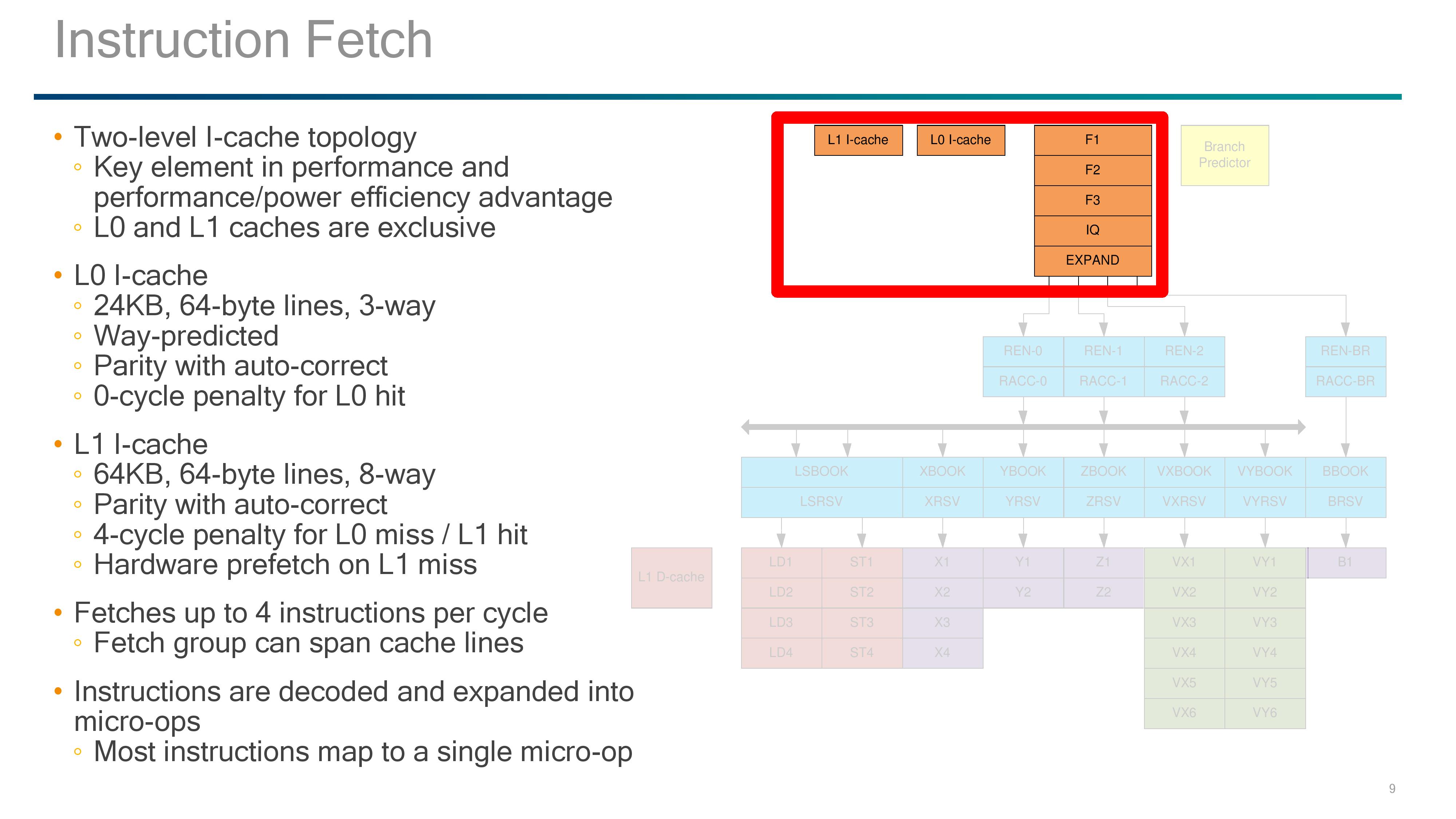
The L1 I-cache is 64KB, which is similar to other ARM architecture core designs, and also uses 64-byte lines but with an 8-way associativity. To software, as the L0 is transparent, the L1 I-cache will show as an 88KB cache. Both the L0 and L1 have parity with auto-correct, and the L1-I has a four cycle penalty on an L0 miss. An L1 miss will initiate a hardware prefetch.
Instructions that go through the fetch end up in the decoders, with the Falkor design supporting 4-issue decode (3 decode + one branch).
The Front End: Rename, Register Access and Reserve (Rename and Dispatch)
It’s worth noting at this point that Qualcomm’s slides seem to make instructions and micro-ops interchangeable at this point, or rather use the term ‘instruction’ where they mean ‘micro-op’.
Direct branches out of the decoder hit their own rename and dispatch pipeline and execution, so the main focus is on the three other decoded micro-ops. Each of these hits the rename and completion buffer, which can support up to 256-entries.
The Qualcomm diagram gets a bit odd here as after the rename/register access stages, the micro-ops hit the out-of-order dispatch buffer. This supports 76 committed micro-ops ready for dispatch or retirement while 128 uncommitted micro-ops can remain in flight, although Qualcomm doesn’t state if these numbers include the Direct Branch decode (it’s worth noting that A73/A75 do not, but A53 does).
The dispatch buffer can push through eight micro-ops per cycle into the reserve stations/issue queues, although only one reserve will serve each execution port, much like a Cortex-A75 design. This means that in order to dispatch eight per cycle, it needs one of each of the execution ports in play. The exceptions to the rule are the two load/store units that use a combined reserve station.


41 Comments
View All Comments
DanNeely - Sunday, August 20, 2017 - link
Mobile CSS needs fixed. Bulleted lists need to wrap, instead of overflowing into horizontal scroll as they currently do on Android.twotwotwo - Sunday, August 20, 2017 - link
The things I most wonder about the chip itself are, how much worse will single-thread speed be, and how much better will throughput/$ be?For serial speed, there's sort of a sliding scale of "good enough"; you can certainly find uses for chips that are slower than Intel's large cores, but as single-thread perf gets worse and worse, more types of app become tricky to run on it because of latency. So you want latency stats for typical enterprisey Java or C# (or, heck, Go) Web app or widely used databases or infrastructure tools. That's also a test of how well compilers and runtimes are tuned for ARMV8, the chip, and live with may cores, but since early customers will have to deal with the ecosystem that exists today, that's reasonable.
For cost-effective throughput I guess we need to have an idea of at least price and power consumption, and parallel benchmarks that will hit bottlenecks a single-threaded one might not, like memory bandwidth. And the toughest comparison is probably against Intel's parts in the same segment, Xeon D and their server Atom chips. Something that makes it harder to win big on throughput/$ is that the CPU's cost and power consumption are only a piece of the total: DRAM, storage, network, and so on account for a lot of it. Also, the big cloud customers Qualcomm wants to win probably aren't paying the same premiums as you and I are to Intel.
Then, aside from questions about the chip itself, there are questions about the ecosystem and customers. There are the questions above of how well toolchains and software are tuned. Maybe the biggest question is whether some big customer will make the leap and do some deployments on lots of slower cores. It might be a strategic long-term bet for some big cloud company that wants more competition in the server chip space, but I bet they have to be willing to lose real money on the effort for a generation or two first.
name99 - Monday, August 21, 2017 - link
Intel sells 28 core CPUs that run at 2.1 GHz (and turbo up to 3.8GHz but see below).Hell, they sell 16 core systems that run at 2.0 GHz and only turbo up to 2.8 GHz.
Remember QC is not TRYING to sell these to amateurs, or even as office servers. They are targeted at data warehouse tasks where the job they're doing will be pretty well defined, and it's expected for the most part that ALL the cores will be running (ie when the work load lightens, you shut down entire dies and then racks, you don't futz around with just shutting down single cores).
For environments like that, turbo'ing is of much less value. QC doesn't have to (and isn't) targeting the entire space of HPC+server+data warehouse, just the part that's a good match to what they're offering.
Threska - Tuesday, August 22, 2017 - link
Well there is the small developer virtualization market like Ansible.prisonerX - Monday, August 21, 2017 - link
A preoccupation with single thread performance is the domain of video game playing teenagers and not terribly important, neither is the "latency" you refer to. This sort of high-core, efficient processor is going to be used where throughput and price/power/performance ratio (ie, all three, not just any one of those), are the key metric.Latency is mostly irrelevant since processing will be stream oriented and bandwidth limited rather than hamstrung by latency (thus features such as memory bandwidth compression). Gimmicks like "turbo" (which should be called by its proper name: "throttling") and favoring single thread performance are counterproductive in this mode. Being able to deploy many CPUs in dense compute nodes is what is required and memory, storage and networking are minor parts here.
I don't know why you think compilers or runtimes is a concern, 99.9% of code is common across archs, so if you've supported a lot of x86 cores your code is going to function well for a lot of ARM cores with a small amount of arch specific configuration. The compilers themselves, namely GCC and LLVM are mature as is their support for ARM.
Finally the new ARM CPUs don't have to beat Intel, just stay roughly competitive, because the one thing the tech industry hates more than a monopoly is a monopoly that has abused its monopoly powers, and Intel is it. Industry is itching for an alternative, and near enough is good enough.
deltaFx2 - Thursday, August 24, 2017 - link
"Industry is itching for an alternative": While this is true, is the industry truly interested in an alternative ISA, or alternative supplier? Because there is one now in the x86 space, and is very competitive, and in some metrics better than Intel. Also, your argument about single threaded performance being irrelevant in servers is false. A famous example of this is a paper in ISCA by google folks arguing in favor of high IPC machines (among other things). They also note that memory bandwidth is not as critical as latency. Now this is specific to google, but in plenty of other cases too, unless you have a very lopsided configuration, bandwidth doesn't get anywhere near saturation. There are also plenty of server users who provide extra cooling capacity to run at higher than base frequencies because it's cheaper than scaling out to more nodes. Obviously, your workloads should scale with freq."Finally the new ARM CPUs don't have to beat Intel," -> change intel to AMD. AMD is hugely motivated to compete on price and has the performance to match intel in many workloads. And AMD's killer app is the 1P system, exactly where Qualcomm intends to go. You also have to add the cost of porting from x86->ARM (recompile, validation, etc). Time is money and employees need to be paid. So the question is, why ARM? More threads/socket? Nope. More memory/socket? Nope. More perf/thread? Probably not based on the architecture described but we'll see. More connectivity then? Nope. Lower absolute power? Maybe. Lower cost? I suspect AMD's MCM design is great for yields. And there's the porting cost if you're not already on ARM.
There's a lot more work to be done and money to be spent before ARM becomes competitive in the mainstream server space. QC has the deep pockets to stick it out, but I am not sure about cavium.
Gc - Sunday, August 20, 2017 - link
Confusing terminology: prefetch vs. fetchPrefetch heuristics predict *future* memory addresses based on past memory access patterns, such as sequential or striding patterns, and try to prefetch the relevant cache lines *before* a miss occurs, attempting to avoid the cache miss or at least reduce the delay. A memory fetch to satisfy a cache miss is not a prefetch.
Slide: "Hardware Prefetch on L1 miss."
Text: "An L1 miss will initiate a hardware prefetch."
The initial fetch is after the miss, so the initial fetch is not a 'prefetch'. I assume this means that it is not only fetching the missed cache line but also triggering the prefetchers to fetch additional cache lines.
Slide: "Hardware data prefetch engine Prefetches for L1, L2, and L3 caches"
Text: "If a miss occurs on the L1-data cache, hardware data prefetchers are used to probe the L2 and L3 caches."
The slide is saying that data is prefetched at all three levels of cache. I'm not sure what the text is saying. Probing refers to querying the caches around the fabric to see which if any holds the requested cache line. This is part of any fetch, not specific to prefetching. Maybe the text is trying to say that the prefetchers not only remember past addresses and predict future addresses, but also remember which cache held past addresses and predicts which cache holds fetched and prefetched addresses?
YoloPascual - Monday, August 21, 2017 - link
Inb4 fanless data centers near the equator.KongClaude - Tuesday, August 22, 2017 - link
'however Samsung does not have much experience with large silicon dies'I don't remember the actual die size for the DEC Alpha's that Samsung fabbed back in the day, the Alpha was a fairly large CPU even by todays standard. Would they have let go of that knowledge or is Alpha being relegated to low-volume/not much experience?
psychobriggsy - Tuesday, August 22, 2017 - link
We should also consider that GlobalFoundries licensed Samsung's 14nm after digging their own 14nm hole and failing to get out of it, and right now AMD are making 486mm^2 Vega dies on that process. The process doesn't have a massive maximum reticle size however, IIRC it's around 700mm^2, whereas TSMC can do just over 800mm^2 on their 16nm.