Analyzing Falkor’s Microarchitecture: A Deep Dive into Qualcomm’s Centriq 2400 for Windows Server and Linux
by Ian Cutress on August 20, 2017 11:00 AM EST- Posted in
- CPUs
- Qualcomm
- Enterprise
- SoCs
- Enterprise CPUs
- ARMv8
- Centriq
- Centriq 2400
Getting Intimate with Falkor: The Front End
So we have to admit that we were surprised by Qualcomm releasing so much information about the pipeline. When we’ve ever asked the mobile CPU team about Krait and Kryo, we usually hit a brick wall, left with a PR answer of a ‘custom core design’ or the guide of ‘protecting our design’. So when Falkor was offered on a plate, we grabbed a knife and a chopstick to devour the soup at hand.
The headline features are as follows:
- Variable length pipelines, 10-15 stage depending on instruction
- 4-wide decode (3 + 1 branch)
- 8-wide out-of-order dispatch
- 8 execution ports
- Micro-op cache / L0 I-cache with Way prediction
- Retire 4/cycle usually (some situations >4)
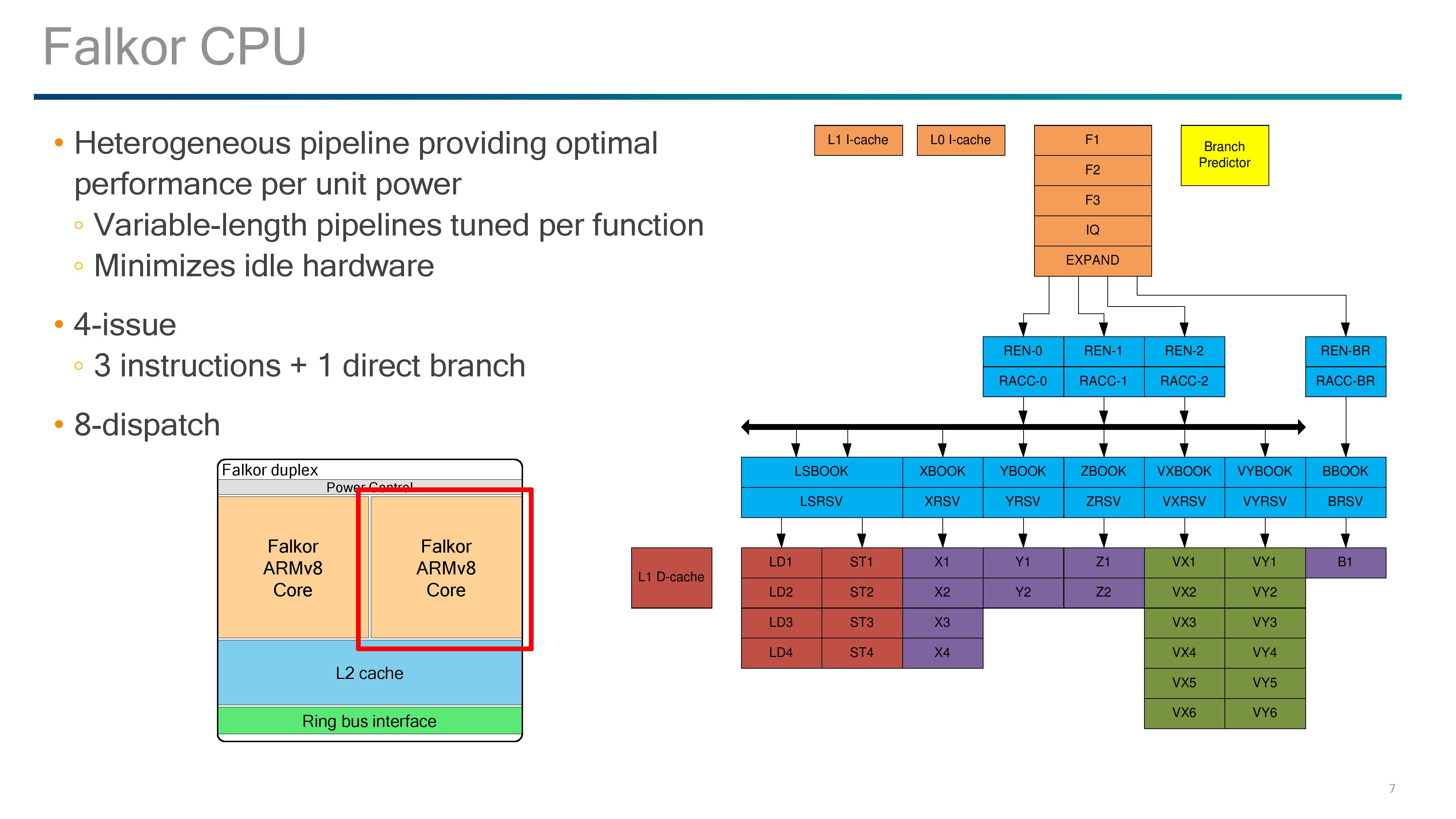
Much like most modern cores and those built on ARM’s instruction sets, pipeline lengths vary for the different execution ports, and Qualcomm states that these are tuned depending on the instruction at play.
Just to add some terminology changes in here: what Intel calls a scheduler, ARM calls an Issue Queue, and Qualcomm calls a ‘Reserve’.
We start with a 4-stage instruction fetch, with the design able to fetch up to four instructions per cycle. These go into a single stage decode that converts the instructions into micro-ops, with most instructions becoming a single micro-op. Branches out of the decode are fed into their own branch rename stage and issue queue, before hitting its own execution port. Micro-ops not fed into the branch stage go into the single-stage rename and single-stage ‘register acccess’ followed by the out-of-order dispatch window.
Up to eight instructions can move into the two-stage Reserves/issue queues, with each execution port having one Reserve except for the load/store units which have a combined Reserve. Loads and stores take 4 stages, ALUs take 2 stages (most) or 4 stages (MUL), while FP and vector pipes take six stages.
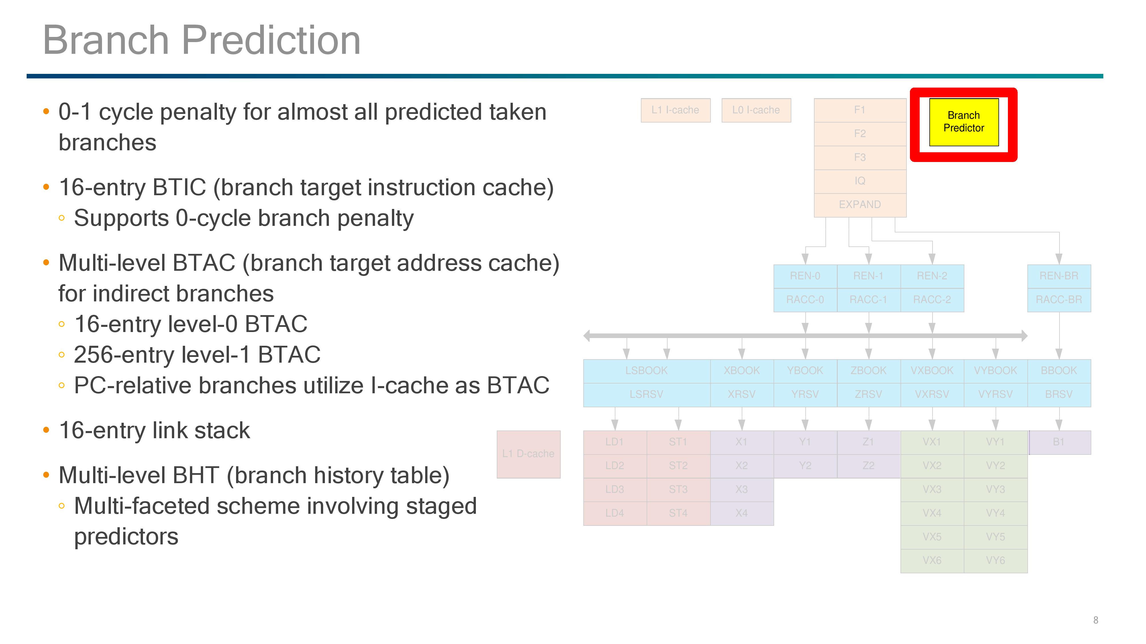
For the fetch stages of the pipeline, Qualcomm doesn’t say much about its prefetch policies here. However we do have information about the branch predictor and L0/L1 caches.
The Front End: Prefetch and Branch Predictor
Qualcomm has implemented a custom branch predictor, and the design gives a 0-1 cycle latency penalty for taking most predicted branches. For instructions, there is a 16-entry branch target instruction cache (BTIC) that supports 0-cycle access, and for addresses there is a two-level branch target address cache (BTAC) for indirect branches: a 16-entry level 0 and a 256-entry level 1. This combines with the 16-entry link stack and multi-level branch history table for predictions.
The Front End: L0/L1 Instruction Caches
The instruction caches are an interesting part of the design, with Qualcomm implementing an L0 I-cache and an L1 I-cache. Qualcomm has implemented L0 caches before, since Krait, but when I initially saw it in this design I instantly thought it looks like a micro-op cache. (in LLVM commits it even states it as a micro-op cache). Normally the test is that if it walks like a micro-op cache and talks like a micro-op cache then it’s a micro-op cache, but the difference here is that rather than storing already-decoded micro-ops, it stores instructions ready to decode.
The special element to the L0 instruction cache here is that it is Way-predicted, meaning that the cache is checked for the instruction as the prefetch also checks the L1. As the L0 is smaller and closer to the event, it offers a 0-cycle latency for any instruction that achieves an L1 hit. The L0 sits at 24 KB, using 64-byte lines and 3-way associativity, but due to the way prediction, the L0 itself is transparent to software and will be seen as part of the L1 cache when metrics probe the size and capability.
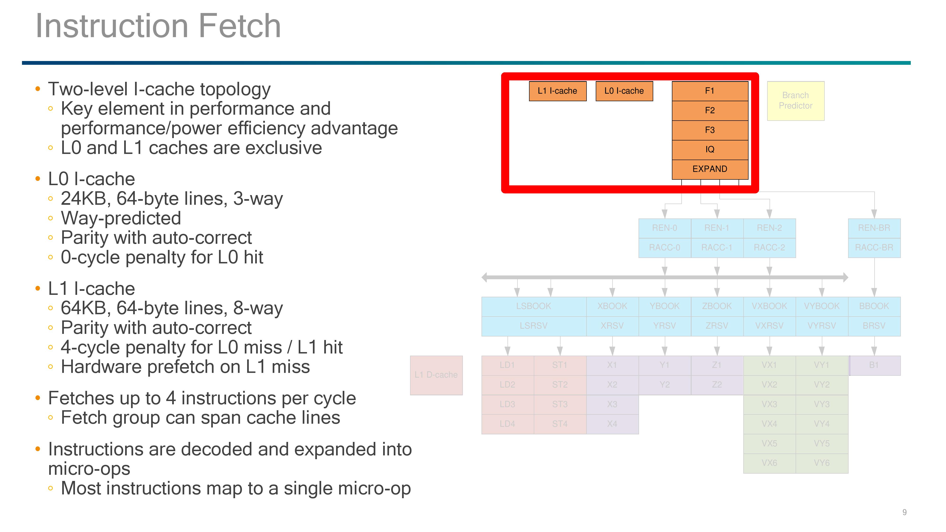
The L1 I-cache is 64KB, which is similar to other ARM architecture core designs, and also uses 64-byte lines but with an 8-way associativity. To software, as the L0 is transparent, the L1 I-cache will show as an 88KB cache. Both the L0 and L1 have parity with auto-correct, and the L1-I has a four cycle penalty on an L0 miss. An L1 miss will initiate a hardware prefetch.
Instructions that go through the fetch end up in the decoders, with the Falkor design supporting 4-issue decode (3 decode + one branch).
The Front End: Rename, Register Access and Reserve (Rename and Dispatch)
It’s worth noting at this point that Qualcomm’s slides seem to make instructions and micro-ops interchangeable at this point, or rather use the term ‘instruction’ where they mean ‘micro-op’.
Direct branches out of the decoder hit their own rename and dispatch pipeline and execution, so the main focus is on the three other decoded micro-ops. Each of these hits the rename and completion buffer, which can support up to 256-entries.
The Qualcomm diagram gets a bit odd here as after the rename/register access stages, the micro-ops hit the out-of-order dispatch buffer. This supports 76 committed micro-ops ready for dispatch or retirement while 128 uncommitted micro-ops can remain in flight, although Qualcomm doesn’t state if these numbers include the Direct Branch decode (it’s worth noting that A73/A75 do not, but A53 does).
The dispatch buffer can push through eight micro-ops per cycle into the reserve stations/issue queues, although only one reserve will serve each execution port, much like a Cortex-A75 design. This means that in order to dispatch eight per cycle, it needs one of each of the execution ports in play. The exceptions to the rule are the two load/store units that use a combined reserve station.


41 Comments
View All Comments
SarahKerrigan - Sunday, August 20, 2017 - link
I seriously doubt SVE is present. As far as I know, Fujitsu is still lined up to be the first SVE user, and it's not like ultra-wide vectors are a massive boost to conventional enterprise servers.Kevin G - Sunday, August 20, 2017 - link
Using SVE requires ARM v8.2A support which this does not appear to have. The ARM v8.2A spec only was announced in January 2016, which isn't enough time to get it implemented into anything that'd be shipping now. Qualcomm could have been working behind the scenes but that would have given them perhaps another year with a spec that could change before formal publishing (i.e. may require some last minute changes right past the design would be tapping out). For a server part, that path would be unwise.SVE was announced a year ago and is far more complex than the v8.2A released due to how it handles execution width. A SVE design right now is a virtual impossibility.
Hurr Durr - Sunday, August 20, 2017 - link
I`d rather read something on x86 thing on ARM that MS and Qualcomm have than this. Much more potential for the real world.Kevin G - Sunday, August 20, 2017 - link
Can we get an editor in here?"For SoC design followers, one might look at this design and think they see similarities with designs such as AMD’s original Bulldozer design from 2011. ... Actually, after writing that last sentence, it is basically a Xeon Phi dual core module."
While perfectly readable, that last paragraph could use a bit of a rewrite due to the last sentence nullifying it. My quick stab at a rewrite:
For SoC followers, the Qualcomm pairs two modules per fabric stop similar to what Intel has implemented in their most recent Xeon Phi chips. Unlike the new grid topology in the Xeon Phi, Qualcomm is using a ring bus akin to what Intel uses on its Xeon E5 and E7 chips. Those thinking that a dual core module would follow AMD's Bulldozer philosophy will be disappointed to learn that no execution resources are shared between the cores, just the L2 cache, power management and bus interface.
The same comparisons and ideas are made but they flow to the reader a bit more logically to me.
FunBunny2 - Sunday, August 20, 2017 - link
-- Unlike the new grid topology in the Xeon Phi, Qualcomm is using a ring bus akin to what Intel uses on its Xeon E5 and E7 chips.I've long wondered how hardware engineers:
1) discover such alternatives
2) decide which one to choose
Is this fundamental math and physics laws, or trial and error? anyone know a readable (for the non-physics major, that is) source?
Kevin G - Monday, August 21, 2017 - link
Topology has been a well studied concept. At a high level, this mimics general networking design closely. The choice of on-die topology is generally at the mercy of engineering trade offs that are unique in this context.The ring bus you get an easy means of scaling the number of units but the trade of is an increase in latency around the ring bus as the numbers go up. Diminishing returns are hit as the numbers increases. With a ring though, individual units on the ring can be radically different sizes on a die as long the links between stops can be roughly the same for timing purposes. A ring bus also permits a relatively predictable latency to reach stops further away, something noteworthy for implementing coherency protocols. Another trade off with the ring design is that it'll always consume power. Nodes that are not in use still need to have the ring stop going to permit data passage through it.
Qualcomm side steps the ring issue a little bit by including two cores per ring stop, thus putting the minimum number of stops at 24. Just like Intel, I suspect on-die IO like PCIe, memory controllers etc. will have their own ring stops. It is not clear if this all on one massive ring bus or like the last generation of E5/E7 high core count chips, several rings are used with discrete bridges between them. Intel never went beyond 16 ring stops in a design.
A grid topology requires far greater engineering resources to implement correctly. Physical size has to be the same for those nodes in the middle of the grid but there is a bit of wiggle room along the perimeter to expand in one of the two dimensions (handy for things like PCIe, memory controllers that have a fixed need per socket). Cache coherency has to account for variable latency between nodes on the grid: there are several paths to between source and destination. The main benefit of a grid though is that scaling is vastly improved as core count increases. Another benefit is that not all the links in between cores needs to be active to move data. This saves power. Due to the ability to route around congested links, the individual links between grid nodes do not necessarily have to be as wide as those on a ring, saving a bit of energy there while maintaining similar aggregate bandwidth. For servers, multi-pathing of data (ie sending it twice) is also possible for increased RAS if an error in transmit is encountered along a particular path. Intel hasn't indicated that they're doing multipathing but could be a feature they add down the road. In the future if chips stacking emerges outside of research labs as feasible, the grid topology can also expand into the 3rd dimension.
The recent Xeon Phi isn't Intel's first attempt at a grid topology. The first publiclly shown off design was there Terascale research chip a decade ago. ( http://www.eetimes.com/document.asp?doc_id=1303295 ) Inter core topology was a major driver of that research effort and the recent Xeon Phi and Xeon series are the result of those efforts. Intel isn't event the first to implement a grid topology. The Compaq/DEC Alpha EV7 did so between sockets and permitted up to 64 sockets in an 8 x 8 grid from the early 2000's. IBM used a grid-like design for their BlueGene super computer designs to move data, though that wasn't cache coherent. There could be earlier instances as those are a few that I know off hand.
FunBunny2 - Monday, August 21, 2017 - link
thanks. much clearer.Ryan Smith - Sunday, August 20, 2017 - link
Thanks!Lord-Bryan - Sunday, August 20, 2017 - link
"So we have to admit that we were surprised by Qualcomm releasing so much information about the pipeline. When we’ve ever asked the mobile CPU team about Krait and Kryo, we usually hit a brick wall, left with a PR answer of a ‘custom core design’ or the guide of ‘protecting our design"Well am not surprised, releasing architectural details of server cpus, has always been an industry norm. It is something they just have to do if they want to be relevant, you can't just sell black boxes worth thousands of dollars to just anyone.
Lord-Bryan - Sunday, August 20, 2017 - link
Plus developers will have to know how the processor works in other to optimize applications for it, Qualcomm is playing with the big boys now, no room for unnecessary pride.