Analyzing Falkor’s Microarchitecture: A Deep Dive into Qualcomm’s Centriq 2400 for Windows Server and Linux
by Ian Cutress on August 20, 2017 11:00 AM EST- Posted in
- CPUs
- Qualcomm
- Enterprise
- SoCs
- Enterprise CPUs
- ARMv8
- Centriq
- Centriq 2400
The SoC: 48 Falcor Cores, DDR4, PCIe
Two decades ago, when processors were a single core with external memory controllers, external caches, and external IO, routing was comparatively easier than what we have today. Now we have many core systems, multiple cache levels of different varieties, more IO than we can shake a stick at, and it all has to communicate with each other in a low power, low latency and high bandwidth way using a variety of interfaces. For the Centriq 2400, Qualcomm is implementing a number of enterprise requirements as well as integrating its own developed fabric.
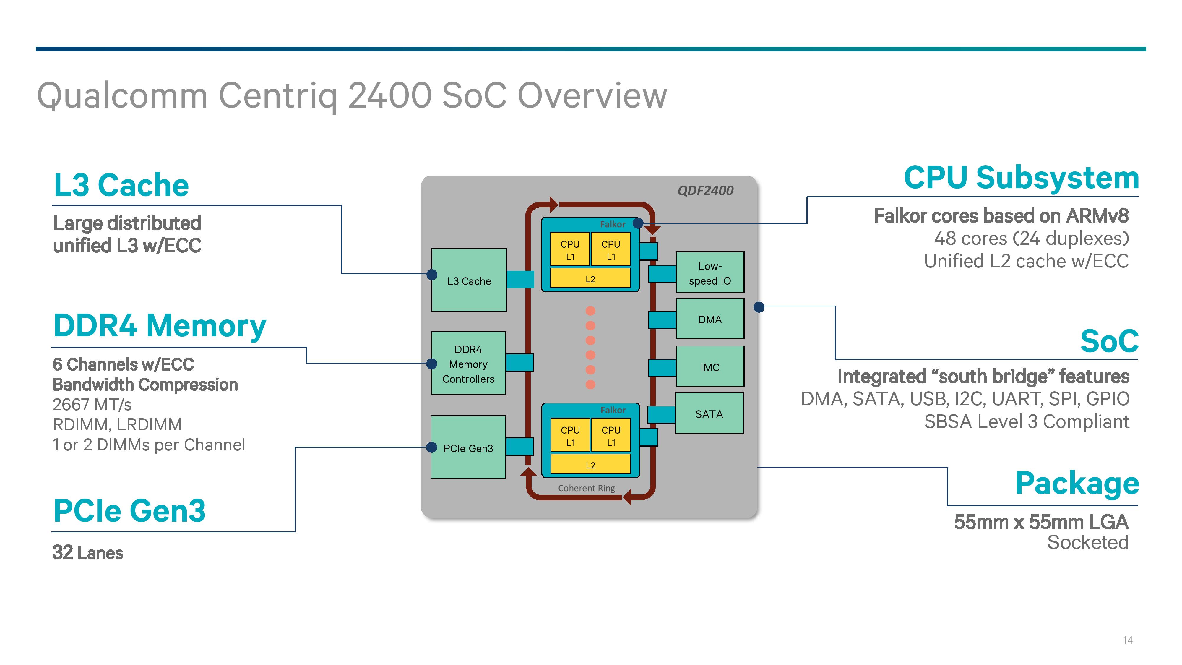
For those that have been following our Intel/AMD coverage of late, we discussed how internal coherent fabrics are changing: Intel has moved from a ring-bus topology to a per-core networking mesh, and AMD uses its scalable Infinity Fabric within a die, between dies, between sockets, and from GPUs to memory. In the mobile space, coherent fabrics like ARMs CCI/CCN are typically all the rage, and ARM allows its partners to modify and tune those IPs as they need to (and most do). Rather than using off-the-shelf IP, Qualcomm has stated that its new interconnect is homegrown.
The Qualcomm System Bus (QSB) is a proprietary protocol based, bidirectional segmented ring bus. While Qualcomm shows a ring bus in the image above, we are told that the segmented ring bus might not exactly look like a ring inside the chip – by creating a segmented core-to-core design, it means the cores might not be in a ring at all, with some elements sprouting from off shoots and cores having more than one direction to travel. If Qualcomm were to share a false-color die shot, this would likely be visible. The QSB also allows for multicast on read as well as shortest path routing, which again sounds more like a mesh based networking implementation. Qualcomm quotes a >250GB/s aggregate bandwidth for the QSB.
On the Fabric is everything the system needs: cores, cache, memory, PCIe and IO.
The Centriq family will implement a pair of Falkor cores into a Falkor ‘Duplex’, where each core with have a private L1 cache and a shared L2 cache with ECC. We’ll cover the Falkor design in the next few pages.
For the L3 cache, Qualcomm has not quoted a size but has said that it will scale with the number of cores on the chip. In the above slide it states that it is a distributed unified cache, which can be confusing. Ultimately the cache is fully accessible from all cores, unless a QoS policy is in play, but the cache is likely segmented to allow for the relevant QoS policy tags to bind certain regions to certain cores/VMs. Despite it saying unified, it means that there will be partitions of the L3 around the QSB interconnect. The L3 will be with ECC as well.
Memory controllers are also accessed from the QSB interconnect, with the Centriq 2400 supporting six memory channels of up to DDR4-2667 at up to 2 DIMMs per channel. Support will include RDIMM and LRDIMM, which would suggest up to 1.5TB of LRDIMM support per socket using 128GB LRDIMMs, similar to Intel’s premium memory offerings.
Connectivity comes via 32 lanes of PCIe 3.0, which falls below that offered by Intel (32-44, fewer when chipset level Quick Assist or 10GbE is being used), AMD (128 PCIe in 1P or 2P), X-Gene 3 (42), or Cavium. We probed Qualcomm on features such as NVMe, NVMe RAID, and fall-over support, although in our limited time briefing there was not time to cover it – we might hear more while we are at Hot Chips this week.
Qualcomm has designed the chip as a true SoC such that it doesn’t need a chipset. We’ve confirmed that this is on-die connectivity, rather than via a multi-chip package add-in. The information we have states that the chip will support the usual array of SATA, USB, I2C, UART, GPIO and DMA, although how much of anything has not been stated.


41 Comments
View All Comments
SarahKerrigan - Sunday, August 20, 2017 - link
"Cavium is the most notable public player using ARM designs in commercial systems so far (there are a number of non-public players focusing on niche scenarios, or whom have little exposure outside of China). The latest design, the Cavium ThunderX2, uses the main A-series core licenses and interconnect license from ARM to provide large numbers of mobile-class CPU cores with as much memory bandwidth and IO as possible."This is not even remotely true. Neither Cavium's cores nor Cavium's interconnect (CCPI predates Cavium's jump to ARM) are ARM IP - they're using an architectural license, *not* IP blocks (or at least, not those ones.) ThunderX uses custom Cavium cores that are between A53 and A57 in performance, while ThunderX2 uses a small number of cores (32) based on the XLP/Vulcan design they bought from Broadcom.
To make that last part more confusing, Cavium initially announced a *different* ThunderX2, which was an enhanced (54-core) derivative of the original ThunderX design. This seems to have been killed when the Vulcan uarch was licensed, or at least has not been heard from since.
Ian Cutress - Sunday, August 20, 2017 - link
That's my fault, I wrote this while flying and thought I had known what is under the hood on ThunderX. Johan actually did a good write up on this, and I'll edit the piece here appropriately.http://www.anandtech.com/show/10353/investigating-...
SarahKerrigan - Sunday, August 20, 2017 - link
"uses the architecture licence for the main A-series core from ARM"That makes even less sense. A-series cores don't factor into it. ThunderX is custom.
name99 - Sunday, August 20, 2017 - link
Is this public knowledge (original ThunderX2 killed, new ThunderX2 based on Vulcan)?I know it's public that (beginning of this year) Cavium acquired Vulcan IP, but I'd not heard anything beyond that. ThunderX2 is supposed to ship Q3 this year (ie RSN...) which to me suggests they're too far along to drop it, and Vulcan will be the basis of ThunderX3.
SarahKerrigan - Sunday, August 20, 2017 - link
Yes. There have been a number of commits to LLVM, etc, indicating that ThunderX2 is now Vulcan. Cf the ThunderX2 LLVM model, which straight-up says "Based on Broadcom Vulcan."I don't know whether the original TX2 design is fully dead or merely mostly dead, but it's pretty obvious at this point that a Vulcan-based TX2 is coming.
SigismundBlack - Sunday, August 20, 2017 - link
Thanks for the info.Denverton rather than 'Denveron'.
Since the C3000 Atom series is cited here re it's also seems worth mentioning AMDs low power server SOCs (e.g. X3421) which likewise feature in recent Moonshot systems and home/SOHO servers.
jameskatt - Sunday, August 20, 2017 - link
The biggest problem I see is if Qualcomm is going to be devoting resources for this project for the long-term. Businesses require stability, predictability, and long-term support. Qualcomm's competitors have been in the business for decades and will be in the business for decades. Qualcomm can't prove they will be in the business for decades to come particularly if they make no money on it.Kevin G - Sunday, August 20, 2017 - link
Qualcomm has been around for awhile so there is stability there. They are new to the ARM server market though because, well after many false starts this market appears to finally be emerging. Even though Qualcomm is just launching this chip, it would be beneficial to them to discuss a roadmap to bring some long term stability to the scene.Wardrive86 - Sunday, August 20, 2017 - link
Surely Qualcomm is using SVE and not regular NEON units. I wish they would expose how wide the units are. I'm very excited they were so open about their architecture. Great write up Ian as well!Dmcq - Sunday, August 20, 2017 - link
I doubt it. SVE is a biggie and was only announced recently, I can't see that Qualcomm would bother risking trying to put it in their first server chip.