The Intel Skylake-X Review: Core i9 7900X, i7 7820X and i7 7800X Tested
by Ian Cutress on June 19, 2017 9:01 AM ESTI Keep My Cache Private
As mentioned in the original Skylake-X announcements, the new Skylake-SP cores have shaken up the cache hierarchy compared to previous generations. What used to be simple inclusive caches have now been adjusted in size, policy, latency, and efficiency, which will have a direct impact on performance. It also means that Skylake-S and Skylake-SP will have different instruction throughput efficiency levels. They could be the difference between chalk and cheese and a result, or the difference between stilton and aged stilton.
Let us start with a direct compare of Skylake-S and Skylake-SP.
| Comparison: Skylake-S and Skylake-SP Caches | ||
| Skylake-S | Features | Skylake-SP |
| 32 KB 8-way 4-cycle 4KB 64-entry 4-way TLB |
L1-D | 32 KB 8-way 4-cycle 4KB 64-entry 4-way TLB |
| 32 KB 8-way 4KB 128-entry 8-way TLB |
L1-I | 32 KB 8-way 4KB 128-entry 8-way TLB |
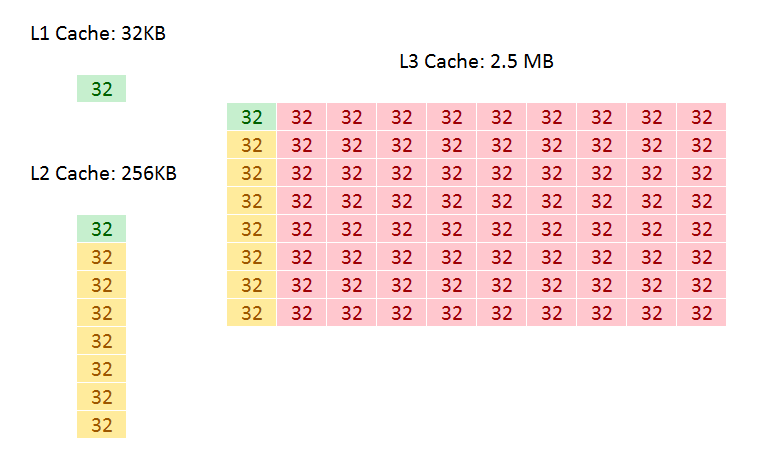
| 256 KB 4-way 11-cycle 4KB 1536-entry 12-way TLB Inclusive |
L2 | 1 MB 16-way 11-13 cycle 4KB 1536-entry 12-way TLB Inclusive |
| < 2 MB/core Up to 16-way 44-cycle Inclusive |
L3 | 1.375 MB/core 11-way 77-cycle Non-inclusive |
The new core keeps the same L1D and L1I cache structures, both implementing writeback 32KB 8-way caches for each. These caches have a 4-cycle access latency, but differ in their access support: Skylake-S does 2x32-byte loads and 1x32-byte store per cycle, whereas Skylake-SP offers double on both.
The big changes are with the L2 and the L3. Skylake-SP has a 1MB private L2 cache with 16-way associativity, compared to the 256KB private L2 cache with 4-way associativity in Skylake-S. The L3 changes to an 11-way non-inclusive 1.375MB/core, from a 20-way fully-inclusive 2.5MB/core arrangement.
That’s a lot to unpack, so let’s start with inclusivity:
Inclusive Caching
An inclusive cache contains everything in the cache underneath it and has to be at least the same size as the cache underneath (and usually a lot bigger), compared to an exclusive cache which has none of the data in the cache underneath it. The benefit of an inclusive cache means that if a line in the lower cache is removed due it being old for other data, there should still be a copy in the cache above it which can be called upon. The downside is that the cache above it has to be huge – with Skylake-S we have a 256KB L2 and a 2.5MB/core L3, meaning that the L2 data could be replaced 10 times before a line is evicted from the L3.
A non-inclusive cache is somewhat between the two, and is different to an exclusive cache: in this context, when a data line is present in the L2, it does not immediately go into L3. If the value in L2 is modified or evicted, the data then moves into L3, storing an older copy. (The reason it is not called an exclusive cache is because the data can be re-read from L3 to L2 and still remain in the L3). This is what we usually call a victim cache, depending on if the core can prefetch data into L2 only or L2 and L3 as required. In this case, we believe the SKL-SP core cannot prefetch into L3, making the L3 a victim cache similar to what we see on Zen, or Intel’s first eDRAM parts on Broadwell. Victim caches usually have limited roles, especially when they are similar in size to the cache below it (if a line is evicted from a large L2, what are the chances you’ll need it again so soon), but some workloads that require a large reuse of recent data that spills out of L2 will see some benefit.
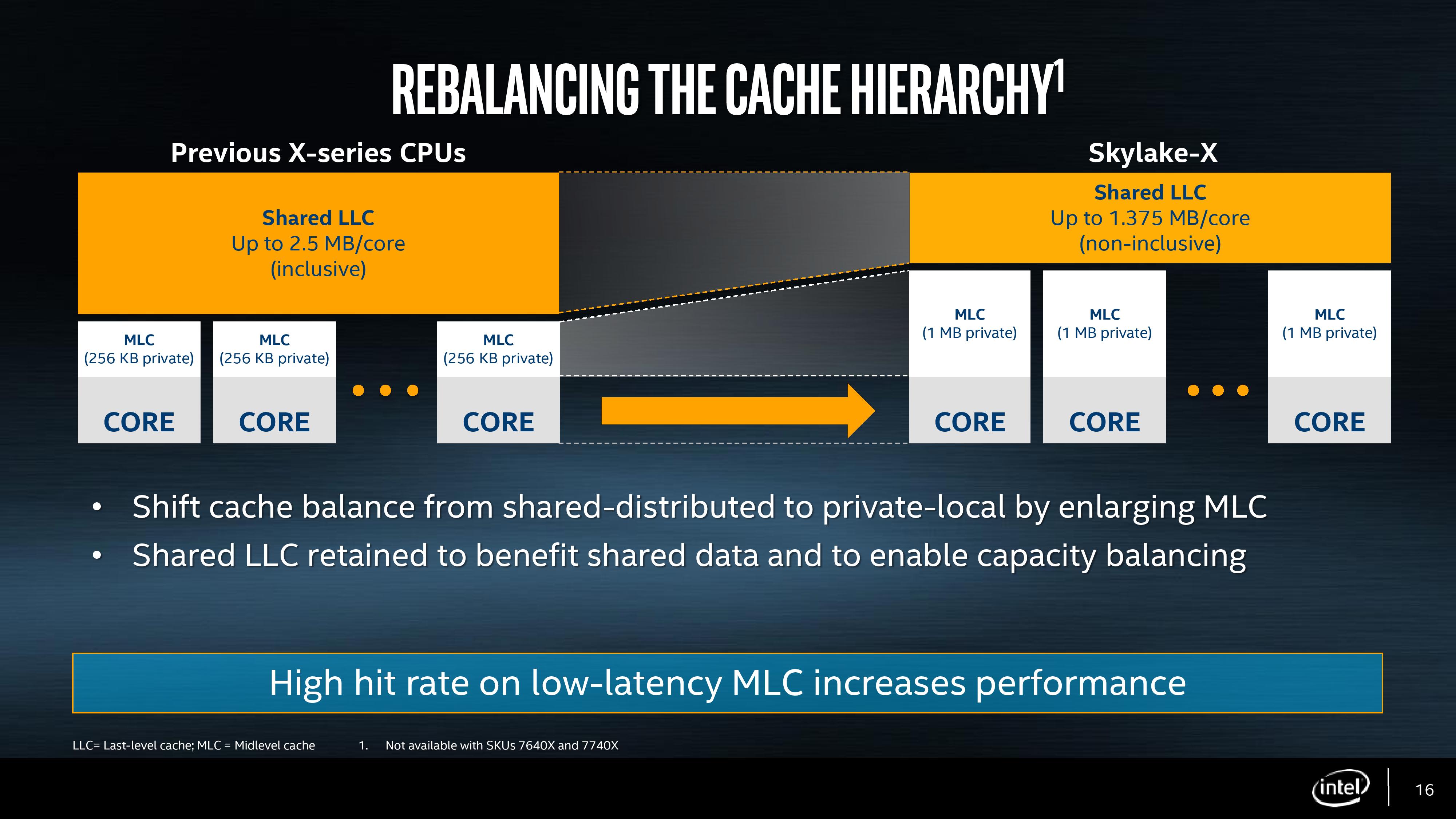
So why move to a victim cache on the L3? Intel’s goal here was the larger private L2. By moving from 256KB to 1MB, that’s a double double increase. A general rule of thumb is that a doubling of the cache increases the hit rate by 41% (square root of 2), which can be the equivalent to a 3-5% IPC uplift. By doing a double double (as well as doing the double double on the associativity), Intel is effectively halving the L2 miss rate with the same prefetch rules. Normally this benefits any L2 size sensitive workloads, which some enterprise environments such as databases can be L2 size sensitive (and we fully suspect that a larger L2 came at the request of the cloud providers).
Moving to a larger cache typically increases latency. Intel is stating that the L2 latency has increased, from 11 cycles to ~13, depending on the type of access – the fastest load-to-use is expected to be 13 cycles. Adjusting the latency of the L2 cache is going to have a knock-on effect given that codes that are not L2 size sensitive might still be affected.
So if the L2 is larger and has a higher latency, does that mean the smaller L3 is lower latency? Unfortunately not, given the size of the L2 and a number of other factors – with the L3 being a victim cache, it is typically used less frequency so Intel can give the L3 less stringent requirements to remain stable. In this case the latency has increased from 44 in SKL-X to 77 in SKL-SP. That’s a sizeable difference, but again, given the utility of the victim cache it might make little difference to most software.
Moving the L3 to a non-inclusive cache will also have repercussions for some of Intel’s enterprise features. Back at the Broadwell-EP Xeon launch, one of the features provided was L3 cache partitioning, allowing limited size virtual machines to hog most of the L3 cache if it was running a mission-critical workflow. Because the L3 cache was more important, this was a good feature to add. Intel won’t say how this feature has evolved with the Skylake-SP core at this time, as we will probably have to wait until that launch to find out.
As a side note, it is worth noting here that Broadwell-E was a 256KB private L2 but 8-way, compared to Skylake-S which was a 256KB private L2 but 4-way. Intel stated that the Skylake-S base core went down in associativity for several reasons, but the main one was to make the design more modular. In this case it means the L2 in both size and associativity are 4x from Skylake-S by design, and shows that there may be 512KB 8-way variants in the future.


264 Comments
View All Comments
Ian Cutress - Monday, June 19, 2017 - link
Didn't get a chance to do overclocking. Testing 5 chips rather than one chip in less than a week (with BIOS issues) means I haven't slept much, and now I'm at a different event half way around the world.Ian Cutress - Monday, June 19, 2017 - link
I should add I have some 5 GHz numbers on Kaby i7. I need to find time to write but I'm fully booked today :(FreckledTrout - Monday, June 19, 2017 - link
Cool! (Pun intended)AnandTechReader2017 - Tuesday, June 20, 2017 - link
Could you also test with Speedshift on/off? Would be interesting how much of an impact it has.lefty2 - Monday, June 19, 2017 - link
One thing that is never covered by any of these reviews is the efficiency of the CPU. If you measure performance of a benchmark, then divide by the the power used in said benchmark, you will see the most efficient CPU by far is the R7 1700. All Intel Skylake-X and Kaby Lake CPUs are far less efficient (also the R7 1800X for that matter).Archie2085 - Monday, June 19, 2017 - link
@BrokenCrayonsOops .. I did not realise how odd it looked.
On a different note . tom's hardware a sister site has done a balanced review including gaming benches.. Still looks like a rushed product :)
Intel has to work on that god awful "TIM"
AnandTechReader2017 - Tuesday, June 20, 2017 - link
Wouldn't trust toms hardware since that fiasco with only Intel chips recommended for everything when the R7 1700 was clearly better a better choice.lordken - Wednesday, July 19, 2017 - link
though they do include ryzen as of next update to their CPU recommend guide. They probably re-evaluated after that shitstorm in their comments :)btw how that fits into your perspective? If they are intel biased how that they did beat i9 quite nicely.
Though I was surprised also that AT didn't talk more about power and heat issues as I did first read Toms article http://www.tomshardware.com/reviews/-intel-skylake... and after I had good lols especially after reading this fabulous line
"Ultimately, we’re looking at power consumption numbers similar to some high-end graphics cards when we start messing with Skylake-X. AMD’s FX-9590X doesn’t even come close to these results"
I came here and was surprised to not read anything here, as thermals and heat looks to be pretty tragic...
If AMD would came up with such space heater it would be all over the place...but since its intel it seems to be no issue.
Kevin G - Monday, June 19, 2017 - link
I would be hesitate to indicate that the memory controller's size is tied the same size as a CPU core for tiling purposes. Intel could easily produce a double wide, half height memory controller and place them at the ends of a column. Intel could also start putting memory controllers on two routers to remove a hop-or-two to cut down on latencies on-die. Ditto for coherecy links and IO controllers. They don't have to be rectangular and the same size of a core for optimal placement.In your mock up of the 5x6 arrangement, there is a lot of wasted space that could be negated if Intel were to re-arrange the dimensions of the IO and memory controllers a bit. Your estimate of a 677 mm^2 is spot on with what you've gone but there is incredible pressure to reduce such huge dies to make them easier to manufacturer. There is simplicity in keeping IO and memory controllers the same size as a core for rapid construction of the entire die but I think the trade off would favor smaller die size here.
Communism - Monday, June 19, 2017 - link
If you are going to post "power consumption" and "power efficiency" graphs/analysis, you need to post the performance from the "power consumption" test itself, or else it's pretty pointless when comparing vastly different CPUs.You mentioned you tested power consumption with prime95.
I'd wager the intel has a hilariously high performance per watt in prime95 as it would likely be using avx2 instructions (and the massive memory bandwidth of the cache as well as the massive memory bandwidth of the main memory/IMC combination if you are using larger dataset option).
I wonder how many hundreds of pages of AMD shill posts that this post will be buried under within hours :P
Oh well, any actual readers should wait for a DigitalFoundry review whenever that happens to come out if you want useful game testing results anyways.