The Intel Skylake-X Review: Core i9 7900X, i7 7820X and i7 7800X Tested
by Ian Cutress on June 19, 2017 9:01 AM ESTMicroarchitecture Analysis
When Intel announced Skylake-S, the Intel Developer Forum soon followed which shed some light on the underlying microarchitecture. While conceptually using the same paradigm since Sandy Bridge, the Core microarchitecture plan has adapted and changed based on tools and capabilities: more buffers, lower latency, libraries optimized for power, throughput, latency and frequency, and support for new instructions plus better ways to do them. One of those marches has been towards better SIMD performance: clustering multiple data entries into a single element and performing the same operation to each of them at once in one go. This has evolved in many forms, from SSE and SSE2 through AVX and AVX2 and now into AVX-512 (technically AVX-512-F + some others). The goal here is that with the right memory subsystem in place, as long as you can keep the units fed with data and instructions, peak throughput for the data can rise substantially compared to a standard INT or FP execution port.
The new core for Skylake-X, technically called the Skylake-SP core from the Intel Xeon Scalable Platform on the enterprise side, beefs up the cores from the previous Broadwell-E HEDT platform all around while also adjusting the cache hierarchy and adding features. As Intel has yet to create separate entries for the new core (we are being told to wait for the enterprise launch for this information), the following info is Skylake-S based with additional information on the new Skylake-SP core.
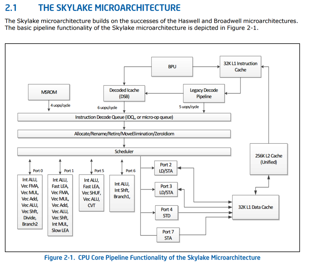
Skylake-S High-Level Core Diagram, from Intel’s Architecture Manual
The base Skylake-S back-end is a six-wide decode using five decoders (four simple, one complex) combined with a 1536 instruction micro-op cache (sometimes called a decoded i-cache) that can support five micro-ops per cycle for instructions that have previously been decoded recently. Instructions that are longer than four micro-ops are served from the MSROM, which can manage 4 micro-ops per cycle. Intel states that the decoders are fed through a more advanced branch prediction unit for Skylake-S over Broadwell-E
These feed into the main instruction queue and out-of-order window, which for Skylake-S was increased to 224 instructions compared to 192 in Haswell. The loop detector in the instruction decode queue can detect loops up to 64 micro-ops per processor, irrespective of hyperthreading. The allocation queue, which also implements rename/retire and other features, follows with 64 entries per thread and is a statically partitioned element of the design (without HT, it will support 128). This feeds into the scheduler, where historically Intel uses a combined scheduler for INT and FP entries. Technically this scheduler can be filled with 180 INT and 168 FP entries, up from 168/168 in Haswell, which can dispatch one micro-op per cycle to each of the eight ports.
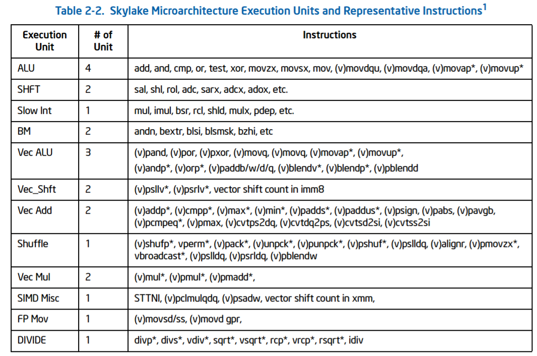
The ports are split as in the diagram, with two load/store units, one dedicated store address unit and one dedicated store data unit. The four ALU ports support a subset of all the ALU features, which Intel states has been balanced over Haswell. The full breakdown is as follows:
- Port 0: ALU/Vec ALU, Vec Shft/Vec Add, Vec Mul/FMA, DIV, Branch2
- Port 1: ALU/Vec ALU/Fast LEA, Vec Shift/Vec Add, Vec Mul/FMA, Slow Int, Slow LEA
- Port 2: Load/Store Address
- Port 3: Load/Store Address
- Port 4: Store Data
- Port 5: ALU/Vec ALU/Fast LEA, Vec Shuffle, (FMA on 10-core SKL-X)
- Port 6: ALU/Shift, Branch1
- Port 7: Store Address
Due to this arrangement, there are only certain combinations of instructions that can be run concurrently – e.g. you can’t put a vector operation across each and every port at once. Intel gives the following guidelines:
Nominally the FMAs on ports 0 and 1 are 256-bit, so in order to drive towards the AVX-512-F these two ports are fused together, similar to how AVX-512-F is implemented in Knights Landing. The six-core and eight-core Skylake-X parts support one fused FMA for AVX-512-F, although the 10-core will support dual 512-bit AVX-512-F ports, which seems to be located on port 5. This means that the 10-core i9-7900X can support 64 SP or 32 DP calculations per cycle, whereas the 8-core/6-core parts can support 32 SP or 16 DP per cycle.
Through the system, up to 72 loads in-flight and 56 stores in-flight are supported, up from 72/42 in Haswell. Some of the instructions have also changed in latency, such as moving to a Radix-1024 divider which brings the division latency from 3-cycles to 5-cycles (we were told that this just helps arrange everything for energy, power and layout). Other instructions typically follow the Skylake-S guidelines, although Intel is holding some information back for the official Skylake-SP launch.
The four load/store related units serve the writeback 32KB L1 Data cache with 8-way associativity and 4-cycle latency. In Skylake-S, this supported two 32-byte reads and one 32-byte store per cycle: in the new Skylake-SP core, this is doubled although Intel only stated that it was ‘128 bytes per cycle read and 64 bytes per cycle write’, which we would assume to mean 2x64B read and 1x64B write. This is backed by an L1D TLB, supporting 64x4KB entries per thread with 4-way associativity.
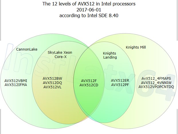
AVX-512? AVX-512-F?
Intel is introducing several variations of the new AVX-512 instruction support, based on the hardware and market segmentation. Ultimately there is one underlying set of AVX-512 instructions supported, and the different variants add different instructions.
AVX-512-F: F for Foundation
AVX-512-BW: Support for 512-bit Word support
AVX-512-CD: Conflict Detect (loop vectorization with possible conflicts)
AVX-512-DQ: More instructions for double/quad math operations
AVX-512-ER: Exponential and Reciprocal
AVX-512-IFMA: Integer Fused Multiply Add with 52-bit precision
AVX-512-PF: Prefetch Instructions
AVX-512-VBMI: Vector Byte Manipulation Instructions
AVX-512-VL: Foundation plus <512-bit vector length support
AVX-512-4VNNIW: Vector Neural Network Instructions Word (variable precision)
AVX-512-4FMAPS: Fused Multiply Accumulation Packed Single precision
We expect there to be FPGA related AVX-512 support in this mix as well at some point.
Nominally these different AVX-512 features are meant to be supported directly by the hardware and enabled therein. It might be possible that the standard AVX-512 block that Intel uses will have features enabled/disabled at a firmware level and users/software may have to be activated/approved to use certain features. Because AVX-512 is designed more for enterprise workloads, these focused instruction sets are unlikely to be part of the consumer workload, but it is worth noting that when someone says ‘AVX-512 support’, you should ask which level of AVX-512 they mean.
We’ve already seen a form of AVX-512 in the latest Xeon Phi processors, Knights Landing (KNL), which support AVX-512-F, AVX-512-CD, AVX-512-ER and AVX-512-PF. The latest KNL chips use 72 Atom Silvermont-class cores arranged as 36 pairs, combined with two AVX-512-units per pair, 16GB of MCDRAM and as much memory bandwidth as you can shake a stick at. The base cores in Knights Landing are slow – 1.2 GHz, but combine that with a potential 32 DP operations per AVX unit, and it’s an impressive machine.
Intel has hinted at future AVX-512 instructions in software development environments, allowing programmers to target certain instructions and get their software ready.
From @InstLatx64
As with previous versions of AVX, when these instructions are needed the CPU will have to reduce frequency in order to maintain stability. In silicon these pathways are densely packed and draw a lot of power, so with AVX instructions, and even more so with AVX-512-F, in order to balance power, voltage drop and the resulting temperature rise, AVX-512-F will run at a lower frequency than AVX/AVX2, and a lower frequency than other core instructions.
Given what we know about the AVX-512 units in Knights Landing, we also know they are LARGE. Intel quoted to us that the AVX-512 register file could probably fit a whole Atom core inside, and from the chip diagrams we have seen, this equates to around 12-15% of a Skylake core minus the L2 cache (or 9-11% with the L2). As seen with Knights Landing, the AVX-512 silicon takes up most of the space.
So with Skylake-X, the cores support F, VL, BW, DQ and CD. This gives a range of potential applications with code moving forward.
What Can Be Done With AVX-512 in a Skylake-SP core?
Intel went into detail about what the AVX-512 units can do and how it is supported.
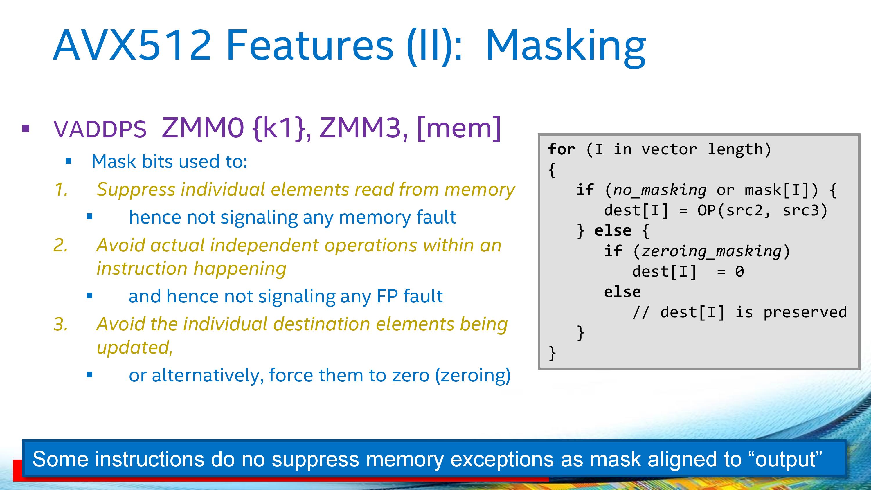
The Skylake-SP core supports separate Mask Registers, which allows Boolean decision operations to be separated into their own silicon rather than take up vector register space (there’s no point storing one bit in a 64-bit register…). This should allow programmers to separate control flow from data flow, especially for such features as encoding as well as reducing energy for logical predicates (performing a check on a mask register consumes less power than a regular register). The AVX-512-F unit supports 512-bit INT/FP calculations from 32 zmm (zmm0 to zmm31) registers, supported by 8 kmask (k0 to k7).

The mask registers can also be used to implement a technique called masking, ensuring individual elements in the main registers can be updated and bypassing potential memory faults, as some instructions (such as VADDPS) do not express memory exceptions and this technique allows the programmer to bypass the known exception event with new data or direct to zero.
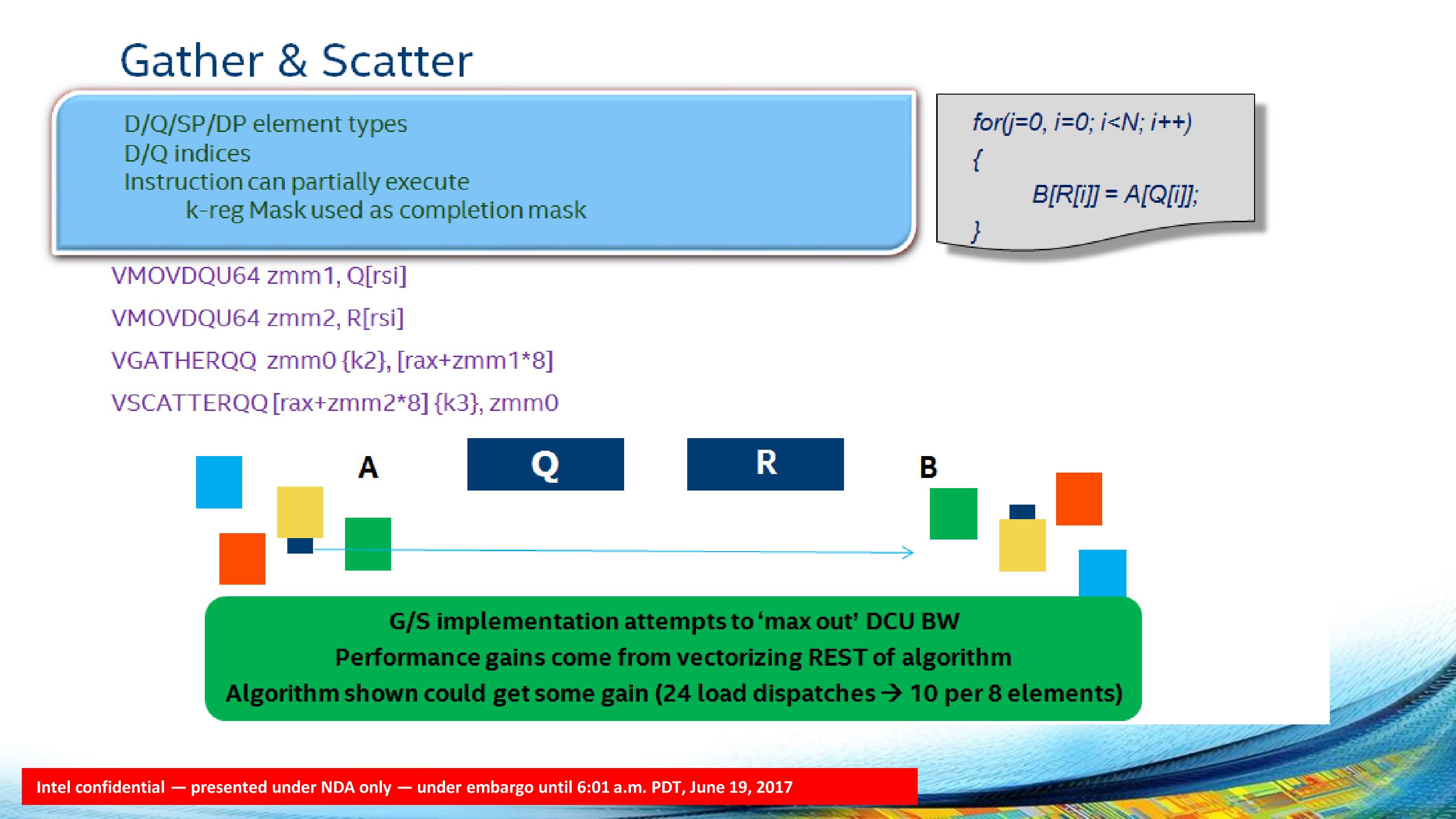
The Skylake-SP core through the AVX-512 also gives native support for 64-bit integers, which allows for basic control functionality to be vectorized and natively supported. Intel cites shift operations and logical operations as the obvious examples, but it also allows vectorization of long integer math as well as pointer codes. Apparently some program software still had edge cases where this function would have to go to x87 in older microarchitectures. The 64-bit support is also important when it comes to gather and scatter operations. Combining this with the masking support allows bandwidth to be maximized in gather/scatter operations and put the emphasis back on other functions in the code.
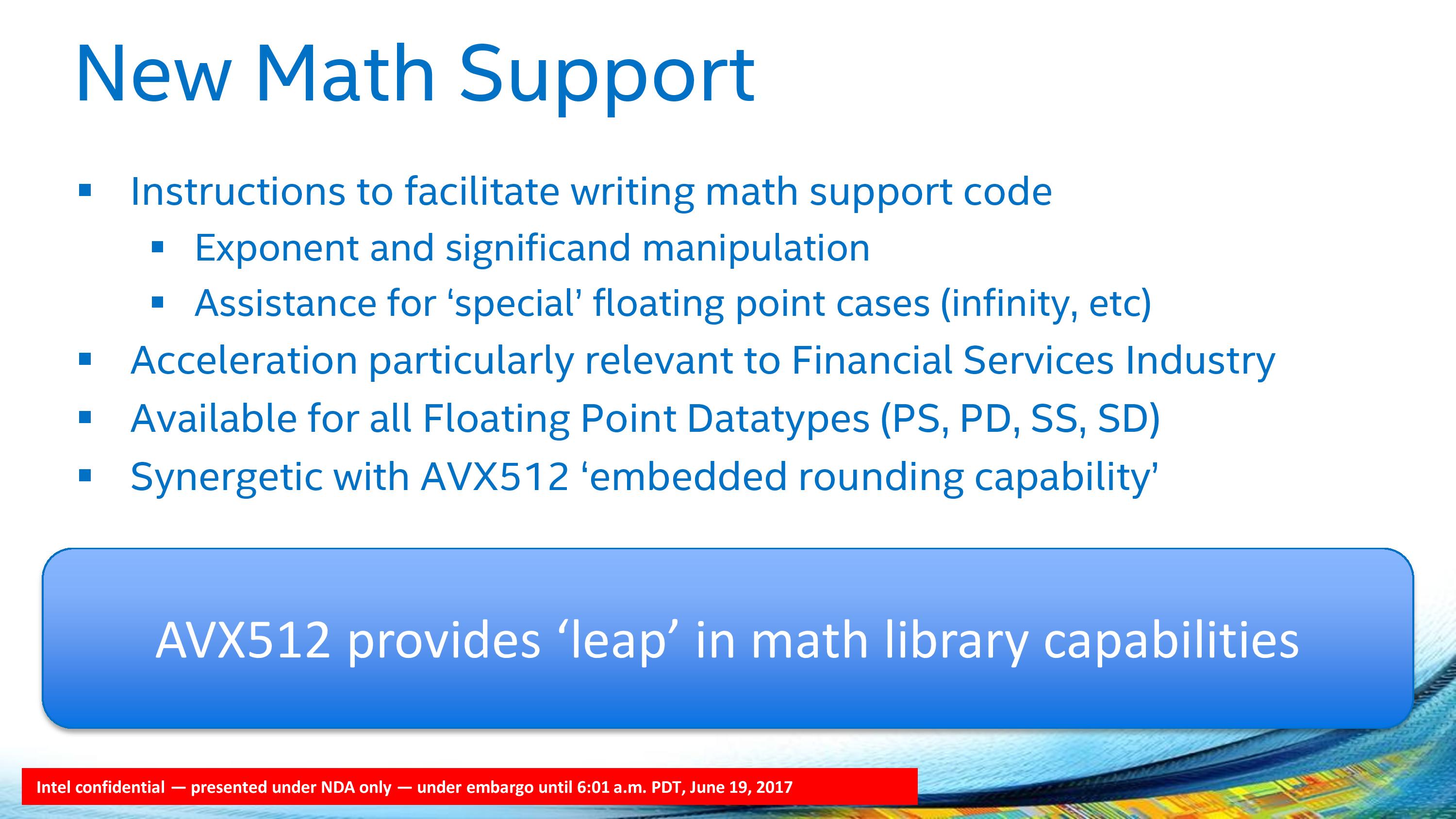
The AVX-512 unit will also allow for additional math support. Scalar, SSE and AVX code can be promoted, but also rounding is embedded with instructions for exponent and significand modification as well as assistance in potential undefined cases (inf, -inf). These new operations can be supported for all FP datatypes (PS, PD, SS, SD), and we are told that this is most important to the financial services industry. We were told that outside financial services, this feature might be of limited use. The AVX-512-F unit will also support packed computations, such as 8-bit and 16-bit dot product support for deep learning, similar to what we have seen with NVIDIA’s tensor cores (8-bit dot products with 32-bit accumulation: SKL-SP can support >40 8-bit multiply-accumulate operations with 32-bit accumulation per core per cycle).
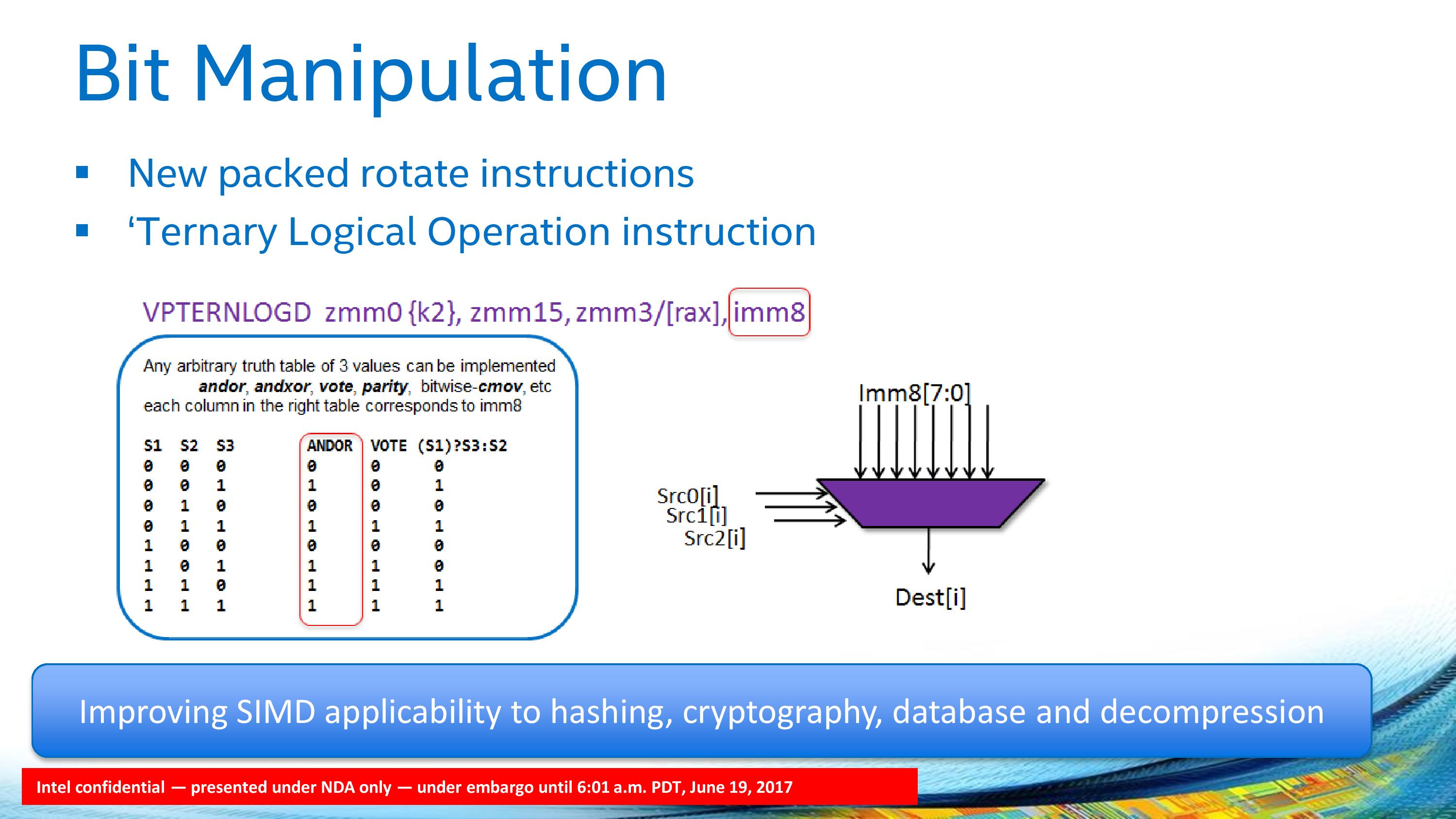
Bit manipulation and packed rotate functions are also given in the new core, allowing an arbitrary three-entry truth table to be implemented in conjunction with the mask registers. This is going to have a big effect for non-ASIC cryptography when the software catches up.
One of the big things that Intel is suggesting about the new AVX-512 unit in the Skylake-SP core is that because of the wide-ranging capabilities, as long as the compilers come on board, it is easier to promote regular code to AVX-512 than it was to SSE/AVX. Fundamentally Intel wants to see the compilers get on board and for the faster throughput of regular software to increase performance. If anyone has recompiled old code under a new compiler and had a performance uplift will know exactly what this might entail (recently POV-Ray recompiled their code for the first time in years, moving from VS2010 to VS2015 – instant 15-25% speed up on the newest microarchitectures).
As mentioned above, the AVX-512 unit is per core, and although more aimed at the enterprise crowd, regular software might take a while to catch up. For anyone on the consumer side who wants to play with AVX-512, it is worth reiterating that there is a separation between the Skylake-X processors: the 6-core and 8-core parts only support one FMA per core, whereas the 10-core supports two FMAs per core.


264 Comments
View All Comments
jjj - Monday, June 19, 2017 - link
The 10 cores die is clearly 320+mm2 not 308mm2. The 308mm figure rounds down the mm based on those GamerNexus pics. From there, you slightly underestimate the size of other 2 die.Sarah Terra - Monday, June 19, 2017 - link
Fair point but what I take from this review is that you are going to be spending pretty much double the cost or higher of ryzen for a proc that will have a 30% larger power envelope if you want higher performance. Intel is scrambling here, well done AMD.jjj - Monday, June 19, 2017 - link
With 8 cores and up, thermal is a big issue when you OC Skylake X.. Power also to some extent.The 6 cores looks interesting vs the 7700k but not so much vs anything else. CPU+mobo gets you north of 600$ and that's a lot. If it had all the PCIe lanes enabled, there would be that but ,while plenty will buy it, it makes no sense to. And ofc there should be a Coffee Lake 6 cores soon , we'll see how it is priced- in consumer 6 cores with 2 mem chans is fine.
More than 6 cores are priced way too high and , if you need many cores, you buy for MT not ST so ST clocks are less relevant.
Intel moving in the same direction as AMD on the cache size front is interesting- larger L2 and smaller L3. Now they have "huge cache and memory latency issues"" just like Ryzen lol.
W/e, Intel's pricing is still far too high and this platform remains of minimal relevance.
ddriver - Monday, June 19, 2017 - link
Funny thou, when Ryzen under-performed in games that was no reason to not publish gaming benches, in fact being the platform's main weakness there was actually emphasis put on that... but when it comes to intel we gotta have special treatment... Let's hear it for objectivity!Granted the 7800X finally brings something of relatively decent value, but still no good reason to justify the purchase unless one insists on an intel product, for the brand, for thunderbolt or hypetane support.
"To play it safe, invest in the Core i9-7900X today."
Really? With Threadripper incoming in a matter of weeks? For less than 1000$ you will get 16 zen cores. It will definitely beat the 7900X by a decent margin in terms of performance, plus the massive I/O capabilities and also ECC support, which I'd say is vital. That just doesn't sound like a honest recommendation. Not surprising in the least.
ddriver - Monday, June 19, 2017 - link
Also, on top of that we have launch prices for Ryzen rather than current prices. Looks like a rather open attempt to diminish AMD's platform value.Ian Cutress - Tuesday, June 20, 2017 - link
We've always posted manufacturer MSRPs in our CPU charts. There has been no official price drop from AMD; if you're seeing lower, it's being run from the distributor level.On the TR issue, we basically haven't tested it and don't know the price. Lots of variables in the air, which is why the words are /if you want to play it safe/. Safe being the key word there.
ddriver - Tuesday, June 20, 2017 - link
Dunno Ian, in my book this sounds more like hasty than safe. The safe thing would be to wait out. Even without the incipient TR launch, early adoption is rather unsafe on its own. As it is, it sounds more like an attempt to dupe people into spending their money on intel in the eve of the launch of a superior value and performance product from a direct (and sole) competitor.It is true that nothing is still officially known about TR, but based on the ryzen marketing strategy and performance we can make safe and accurate speculations. I expect to see the top TR chip launched at 999$ offering at the very least 30% of performance advantage over the 7900X in a similar or slightly higher thermal budget, of course in workloads that can scale nicely up with the core count.
Comparing the 7900X to the 1800X, we have ~35% performance advantage for 205% the price and 150% the power usage. Based on that, it is a safe bet that TR is going to shine.
fanofanand - Monday, June 26, 2017 - link
Ian is a scientist, the less guessing the better. Give him an opportunity to review TR before giving suggestions. Doesn't that seem fair?t.s - Tuesday, June 20, 2017 - link
Play it safe? Really?? Please. As if everyone in this world's stupid.Ranger1065 - Wednesday, June 21, 2017 - link
There has never been a better time to give Intel the middle finger.