The Intel Skylake-X Review: Core i9 7900X, i7 7820X and i7 7800X Tested
by Ian Cutress on June 19, 2017 9:01 AM ESTI Keep My Cache Private
As mentioned in the original Skylake-X announcements, the new Skylake-SP cores have shaken up the cache hierarchy compared to previous generations. What used to be simple inclusive caches have now been adjusted in size, policy, latency, and efficiency, which will have a direct impact on performance. It also means that Skylake-S and Skylake-SP will have different instruction throughput efficiency levels. They could be the difference between chalk and cheese and a result, or the difference between stilton and aged stilton.
Let us start with a direct compare of Skylake-S and Skylake-SP.
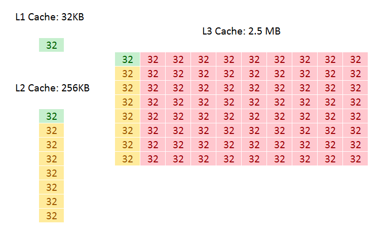
| Comparison: Skylake-S and Skylake-SP Caches | ||
| Skylake-S | Features | Skylake-SP |
| 32 KB 8-way 4-cycle 4KB 64-entry 4-way TLB |
L1-D | 32 KB 8-way 4-cycle 4KB 64-entry 4-way TLB |
| 32 KB 8-way 4KB 128-entry 8-way TLB |
L1-I | 32 KB 8-way 4KB 128-entry 8-way TLB |
| 256 KB 4-way 11-cycle 4KB 1536-entry 12-way TLB Inclusive |
L2 | 1 MB 16-way 11-13 cycle 4KB 1536-entry 12-way TLB Inclusive |
| < 2 MB/core Up to 16-way 44-cycle Inclusive |
L3 | 1.375 MB/core 11-way 77-cycle Non-inclusive |
The new core keeps the same L1D and L1I cache structures, both implementing writeback 32KB 8-way caches for each. These caches have a 4-cycle access latency, but differ in their access support: Skylake-S does 2x32-byte loads and 1x32-byte store per cycle, whereas Skylake-SP offers double on both.
The big changes are with the L2 and the L3. Skylake-SP has a 1MB private L2 cache with 16-way associativity, compared to the 256KB private L2 cache with 4-way associativity in Skylake-S. The L3 changes to an 11-way non-inclusive 1.375MB/core, from a 20-way fully-inclusive 2.5MB/core arrangement.
That’s a lot to unpack, so let’s start with inclusivity:
Inclusive Caching
An inclusive cache contains everything in the cache underneath it and has to be at least the same size as the cache underneath (and usually a lot bigger), compared to an exclusive cache which has none of the data in the cache underneath it. The benefit of an inclusive cache means that if a line in the lower cache is removed due it being old for other data, there should still be a copy in the cache above it which can be called upon. The downside is that the cache above it has to be huge – with Skylake-S we have a 256KB L2 and a 2.5MB/core L3, meaning that the L2 data could be replaced 10 times before a line is evicted from the L3.
A non-inclusive cache is somewhat between the two, and is different to an exclusive cache: in this context, when a data line is present in the L2, it does not immediately go into L3. If the value in L2 is modified or evicted, the data then moves into L3, storing an older copy. (The reason it is not called an exclusive cache is because the data can be re-read from L3 to L2 and still remain in the L3). This is what we usually call a victim cache, depending on if the core can prefetch data into L2 only or L2 and L3 as required. In this case, we believe the SKL-SP core cannot prefetch into L3, making the L3 a victim cache similar to what we see on Zen, or Intel’s first eDRAM parts on Broadwell. Victim caches usually have limited roles, especially when they are similar in size to the cache below it (if a line is evicted from a large L2, what are the chances you’ll need it again so soon), but some workloads that require a large reuse of recent data that spills out of L2 will see some benefit.
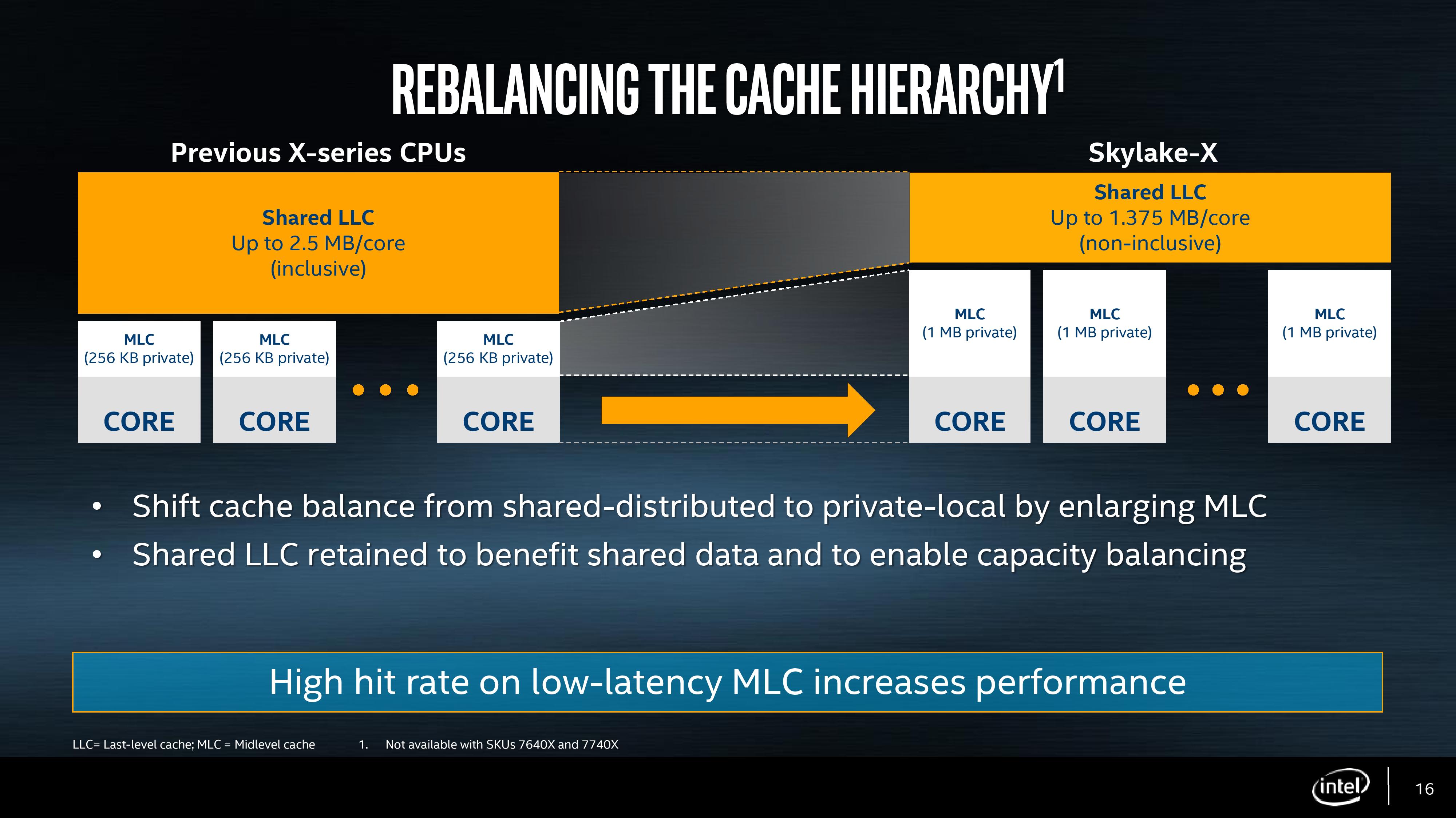
So why move to a victim cache on the L3? Intel’s goal here was the larger private L2. By moving from 256KB to 1MB, that’s a double double increase. A general rule of thumb is that a doubling of the cache increases the hit rate by 41% (square root of 2), which can be the equivalent to a 3-5% IPC uplift. By doing a double double (as well as doing the double double on the associativity), Intel is effectively halving the L2 miss rate with the same prefetch rules. Normally this benefits any L2 size sensitive workloads, which some enterprise environments such as databases can be L2 size sensitive (and we fully suspect that a larger L2 came at the request of the cloud providers).
Moving to a larger cache typically increases latency. Intel is stating that the L2 latency has increased, from 11 cycles to ~13, depending on the type of access – the fastest load-to-use is expected to be 13 cycles. Adjusting the latency of the L2 cache is going to have a knock-on effect given that codes that are not L2 size sensitive might still be affected.
So if the L2 is larger and has a higher latency, does that mean the smaller L3 is lower latency? Unfortunately not, given the size of the L2 and a number of other factors – with the L3 being a victim cache, it is typically used less frequency so Intel can give the L3 less stringent requirements to remain stable. In this case the latency has increased from 44 in SKL-X to 77 in SKL-SP. That’s a sizeable difference, but again, given the utility of the victim cache it might make little difference to most software.
Moving the L3 to a non-inclusive cache will also have repercussions for some of Intel’s enterprise features. Back at the Broadwell-EP Xeon launch, one of the features provided was L3 cache partitioning, allowing limited size virtual machines to hog most of the L3 cache if it was running a mission-critical workflow. Because the L3 cache was more important, this was a good feature to add. Intel won’t say how this feature has evolved with the Skylake-SP core at this time, as we will probably have to wait until that launch to find out.
As a side note, it is worth noting here that Broadwell-E was a 256KB private L2 but 8-way, compared to Skylake-S which was a 256KB private L2 but 4-way. Intel stated that the Skylake-S base core went down in associativity for several reasons, but the main one was to make the design more modular. In this case it means the L2 in both size and associativity are 4x from Skylake-S by design, and shows that there may be 512KB 8-way variants in the future.


264 Comments
View All Comments
halcyon - Monday, June 19, 2017 - link
Thank you for the review. The AVX512 situation was a bit unclear. Which models have which AVX512 support of the now released chips (and the future, yet to be released chips). It would be interesting to see AVX512 specific article once the chips are out and we have (hopefully) some useful AVX512-optimized software (like encoding).For myself, decision is easy now to postpone, until ThreadRipper is out. The thermals are just out of whack and for my workloads, the price is not justified. Here's hoping Threadripper can deliver more for same price or less.
Bulat Ziganshin - Monday, June 19, 2017 - link
all skl-x has avx-512 support. i9 cpus has double fma512 engines, but as i guess - that's only difference, i.e. remaining 512-bit commands (such as integer operations) will have the same throughput on i7 and i9but i may be wrong and it will be really very ibteresting to check throughput of all other operatins. probably Anand can't do that and we will need to wait until Agner Fog will reach these spus
halcyon - Monday, June 19, 2017 - link
Thanks. Many questions remain: AVX512F vs AVX512BW, which are supported now, which in the future? What is the difference? How does it compare to Knights Landing? Are number of AVX units tied to number of cores? What is the speed differential in AVX512 loads? What is the oc limitation from AVX512 support? etc.nevcairiel - Monday, June 19, 2017 - link
Those Knights Landing/Knights Mill specific AVX512 instructions are actually very specific to the work-loads you would see on such a specialized CPU. The instructions chosen for Skylake-X and future Cannon Lake more closely match what we already know from AVX/AVX2.For the "types" of AVX512, basically its split into several sub-instruction sets, all containing different instructions. AVX512 will always include F, because thats the basis for everything (instruction encoding, 512-bit registers, etc). BW/DQ include the basic instructions we know from AVX/AVX2, just for 512-bit registers. SKL-X supports all of F, CD, BW, DQ, VL.
Wikipedia on AVX-512 has some more info on the different feature sets of AVX-512:
https://en.wikipedia.org/wiki/AVX-512
Its generally safe to just ignore the Knights Landing specific instructions. They are very specific to the workloads on those systems. The AVX-512 subset used for Xeon "Purley" and SKL-X is more inline with the AVX/AVX2 instructions we had before - just bigger.
For software, x264 for example already got some AVX512 optimizations over the recent weeks, it might be interesting to test how much that helps once all the launch dust settles.
halcyon - Tuesday, June 20, 2017 - link
Thank you very much!satai - Monday, June 19, 2017 - link
Any idea, why is Intel so much better at Chrome compilation?IanHagen - Monday, June 19, 2017 - link
I'd like to know that as well. Ryzen does particularly fine compiling the Linux Kernel, for example, as seen in: http://www.phoronix.com/scan.php?page=article&...tamalero - Monday, June 19, 2017 - link
Optimizations?I still remember when Intel actively paid some software developers to block multicore and threading on AMD chips to boast about "more performance" during the athlon X2 days.
johnp_ - Tuesday, June 20, 2017 - link
It's just the enterprise parts. Kaby Lake S is behind Ryzen:http://www.anandtech.com/show/11244/the-amd-ryzen-...
Gothmoth - Monday, June 19, 2017 - link
if powerdraw and heat would not be so crazy i would buy the 8 core today.but more than the price these heat issues are a concern for me.. i like my systems to be quiet....