Sizing Up Servers: Intel's Skylake-SP Xeon versus AMD's EPYC 7000 - The Server CPU Battle of the Decade?
by Johan De Gelas & Ian Cutress on July 11, 2017 12:15 PM EST- Posted in
- CPUs
- AMD
- Intel
- Xeon
- Enterprise
- Skylake
- Zen
- Naples
- Skylake-SP
- EPYC
Intel Expanding the Chipset: 10 Gigabit Ethernet and QuickAssist Technology
The refresh strategy from Intel on the chipset side has an ultra-long cadence. In recent memory, Intel’s platform launches are designed to support two generations of processor release, and in that time there is typically no chipset update, leaving the platform controller hub semi-static for functionality for usually three years. This is compared to the consumer side, where new chipsets are launched with every new CPU generation, with bigger jumps coming every couple of years. For the new launch today, Intel pushing the enterprise chipset ahead in a new direction.
The point of the chipset previously was to provide some basic IO support in the form of SATA/SAS ports, some USB ports, and a few PCIe lanes for simple controllers like USB 3.0, Gigabit Ethernet, or perhaps an x4 PCIe slot for a non-accelerator type card. The new chipsets, part of the C620 family codenamed Lewisburg, are designed to assist with networking, cryptography, and act more like a PCIe switch with up to 20 PCIe 3.0 lane support.
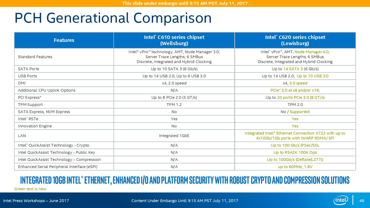
The headline features that matter most is the upgrade in DMI connection to the chipset, upgraded from DMI 2.0 to DMI 3.0 to match the consumer platforms, having those 20 PCIe 3.0 lanes from the chipset, and also the new feature under CPU Uplink.
For the new generation of Lewisburg chipsets, if an OEM requires that a platform has access to a cryptography engine or 10 Gigabit Ethernet, then they can attach 8 or 16 lanes from the processor into the chipset via this CPU Uplink port. Depending on which model of chipset is being used, this can provide up to four 10 GbE ports with iWARP RDMA, or up to 100 GB/s IPSec/SSL of QuickAssist support.
Intel will offer seven different versions of the chipset, varying in 10G and QAT support, but also varying in TDP:
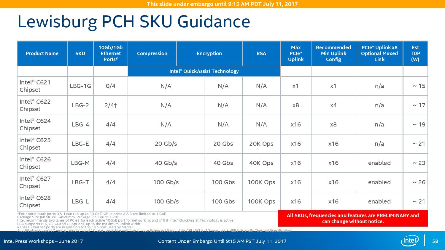
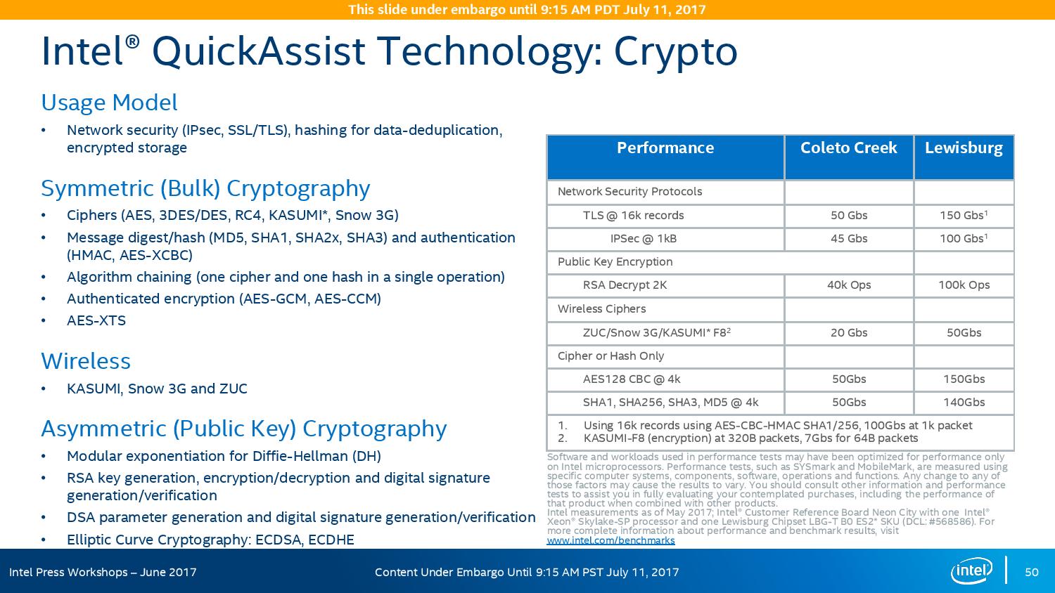
On the cryptography side, Intel has previously sold add-in PCIe cards for QuickAssist, but is now moving it onto the systems directly. By adding it into the chipset, it can be paired with the Ethernet traffic and done in-situ, and specifically Intel points to bulk cryptography (150 Gb/s AES256/SHA256), Public Key Encryption (100k ops of RSA2048) and compression (100+ Gb/s deflate).
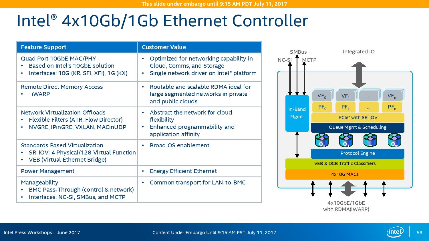
With the GbE, Intel has designed this to be paired with the X722 PHY, and supports network virtualization, traffic shaping, and supports Intel’s Data Plane Development Kit for advanced packet forwarding.
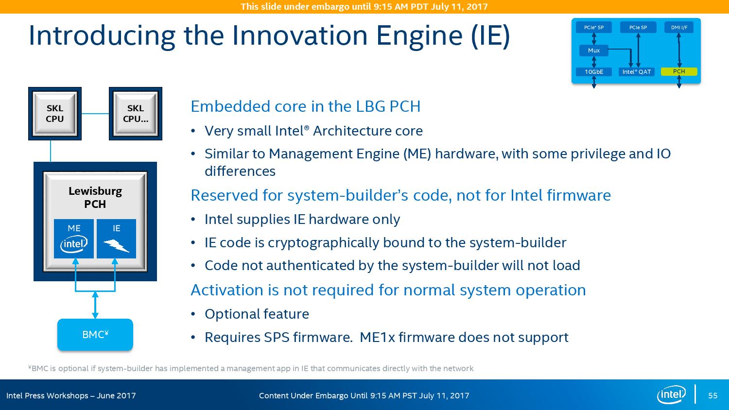
The chipset will also include a new feature called Intel’s Innovation Engine, giving a small embedded core into the PCH which mirrors Intel’s Management Engine but is designed for system-builders and integrators. This allows specialist firmware to manage some of the capabilities of the system on top of Intel’s ME, and is essentially an Intel Quark x86 core with 1.4MB SRAM.
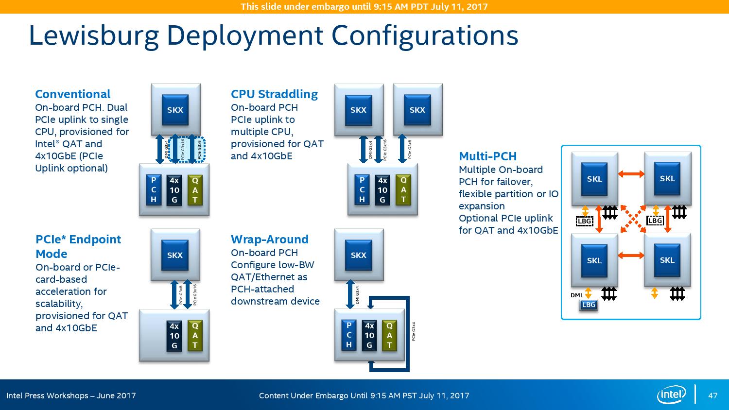
The chipsets are also designed to be supported between different CPUs within the same multi-processor system, or for a system to support multiple chipsets at once as needed.


219 Comments
View All Comments
oldlaptop - Thursday, July 13, 2017 - link
Why on earth is gcc -Ofast being used to mimic "real-world", non-"aggressively optimized"(!) conditions? This is in fact the *most* aggressive optimization setting available; it is very sensitive to the exact program being compiled at best, and generates bloated (low priority on code size) and/or buggy code at worst (possibly even harming performance if the generated code is so big as to harm cache coherency). Most real-world software will be built with -O2 or possibly -Os. I can't help but wonder why questions weren't asked when SPEC complained about this unwisely aggressive optimization setting...peevee - Thursday, July 13, 2017 - link
"added a second full-blown 512 bit AVX-512 unit. "Do you mean "added second 256 ALU, which in combination with the first one implements full 512-bit AVX-512 unit"?
peevee - Thursday, July 13, 2017 - link
"getting data from the right top node to the bottom left node – should demand around 13 cycles. And before you get too concerned with that number, keep in mind that it compares very favorably with any off die communication that has to happen between different dies in (AMD's) Multi Chip Module (MCM), with the Skylake-SP's latency being around one-tenth of EPYC's."1/10th? Asking data from L3 on the chip next to it will take 130 (or even 65 if they are talking about averages) cycles? Does not sound realistic, you can request data from RAM at similar latencies already.
AmericasCup - Friday, July 14, 2017 - link
'For enterprises with a small infrastructure crew and server hardware on premise, spending time on hardware tuning is not an option most of the time.'Conversely, our small crew shop has been tuning AMD (selected for scalar floating point operations performance) for years. The experience and familiarity makes switching less attractive.
Also, you did all this in one week for AMD and two weeks for Intel? Did you ever sleep? KUDOS!
JohanAnandtech - Friday, July 21, 2017 - link
Thanks for appreciating the effort. Luckily, I got some help from Ian on Tuesday. :-)AntonErtl - Friday, July 14, 2017 - link
According to http://www.anandtech.com/show/10158/the-intel-xeon... if you execute just one AVX256 instruction on one core, this slows down the clocks of all E5v4 cores on the same socket for at least 1ms. Somewhere I read that newer Xeons only slow down the core that executes the AVX256 instruction. I expect that it works the same way for AVX512, and yes, this means that if you don't have a load with a heavy proportion of SIMD instructions, you are better off with AVX128 or SSE. The AMD variant of having only 128-bit FPUs and no clock slowdown looks better balanced to me. It might not win Linpack benchmark competitions, but for that one uses GPUs anyway these days.wagoo - Sunday, July 16, 2017 - link
Typo on the CLOSING THOUGHTS page: "dual Silver Xeon solutions" (dual socket)Great read though, thanks! Can finally replace my dual socket shanghai opteron home server soon :)
Chaser - Sunday, July 16, 2017 - link
AMD's CPU future is looking very promising!bongey - Tuesday, July 18, 2017 - link
EPYC power consumption is just wrong. Somehow you are 50W over what everyone else is getting at idle. https://www.servethehome.com/amd-epyc-7601-dual-so...Nenad - Thursday, July 20, 2017 - link
Interesting SPECint2006 results:- Intel in their slide #9 claims that Intel 8160 is 2% faster than EPYC 7601
- Anandtech in article tests that EPYC 7601 is 42% faster than Intel 8176
Those two are quite different, even if we ignore that 8176 should be faster than 8160. In other words, those Intel test results look very suspicious.