Sizing Up Servers: Intel's Skylake-SP Xeon versus AMD's EPYC 7000 - The Server CPU Battle of the Decade?
by Johan De Gelas & Ian Cutress on July 11, 2017 12:15 PM EST- Posted in
- CPUs
- AMD
- Intel
- Xeon
- Enterprise
- Skylake
- Zen
- Naples
- Skylake-SP
- EPYC
Intel Expanding the Chipset: 10 Gigabit Ethernet and QuickAssist Technology
The refresh strategy from Intel on the chipset side has an ultra-long cadence. In recent memory, Intel’s platform launches are designed to support two generations of processor release, and in that time there is typically no chipset update, leaving the platform controller hub semi-static for functionality for usually three years. This is compared to the consumer side, where new chipsets are launched with every new CPU generation, with bigger jumps coming every couple of years. For the new launch today, Intel pushing the enterprise chipset ahead in a new direction.
The point of the chipset previously was to provide some basic IO support in the form of SATA/SAS ports, some USB ports, and a few PCIe lanes for simple controllers like USB 3.0, Gigabit Ethernet, or perhaps an x4 PCIe slot for a non-accelerator type card. The new chipsets, part of the C620 family codenamed Lewisburg, are designed to assist with networking, cryptography, and act more like a PCIe switch with up to 20 PCIe 3.0 lane support.
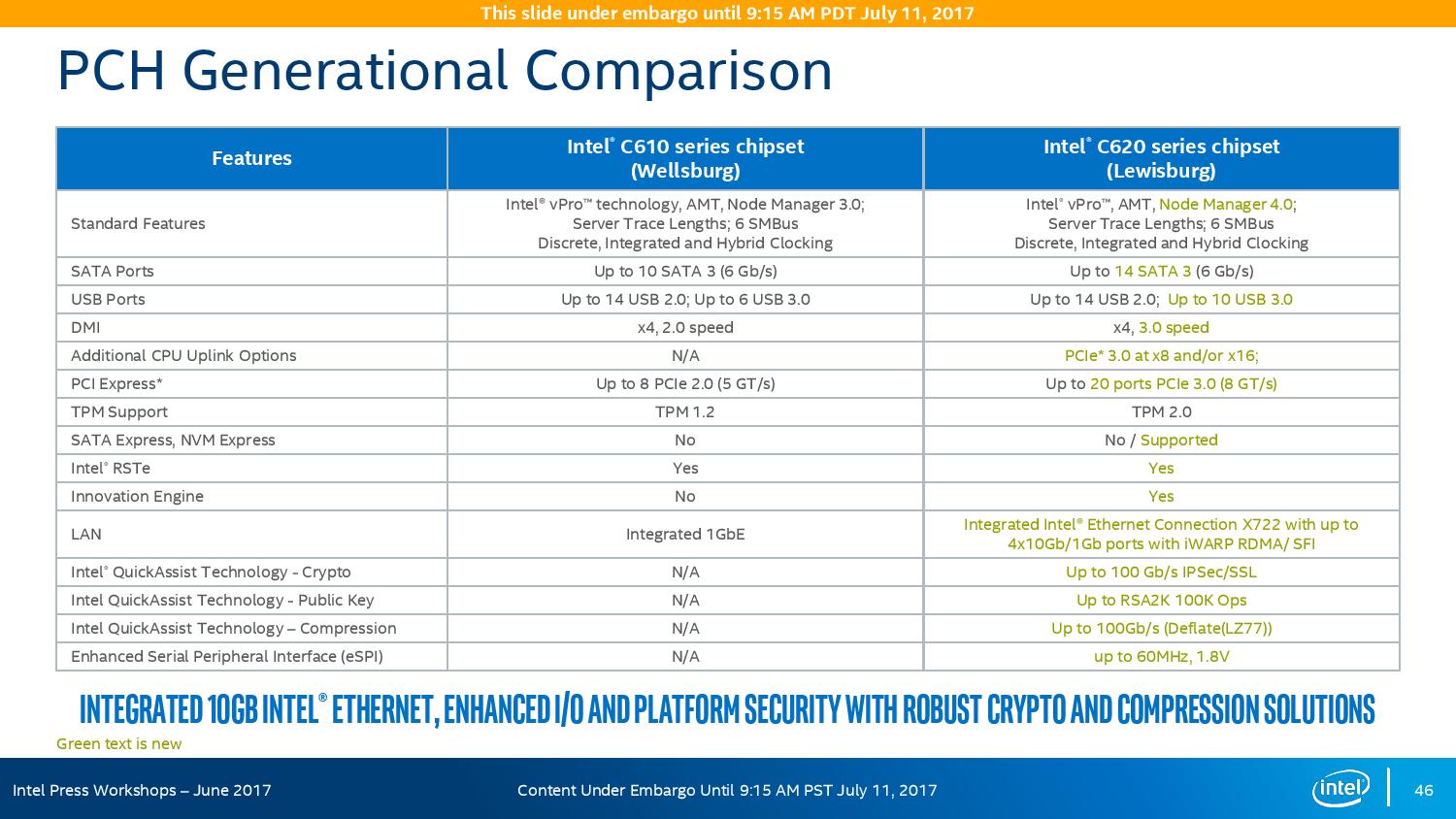
The headline features that matter most is the upgrade in DMI connection to the chipset, upgraded from DMI 2.0 to DMI 3.0 to match the consumer platforms, having those 20 PCIe 3.0 lanes from the chipset, and also the new feature under CPU Uplink.
For the new generation of Lewisburg chipsets, if an OEM requires that a platform has access to a cryptography engine or 10 Gigabit Ethernet, then they can attach 8 or 16 lanes from the processor into the chipset via this CPU Uplink port. Depending on which model of chipset is being used, this can provide up to four 10 GbE ports with iWARP RDMA, or up to 100 GB/s IPSec/SSL of QuickAssist support.
Intel will offer seven different versions of the chipset, varying in 10G and QAT support, but also varying in TDP:
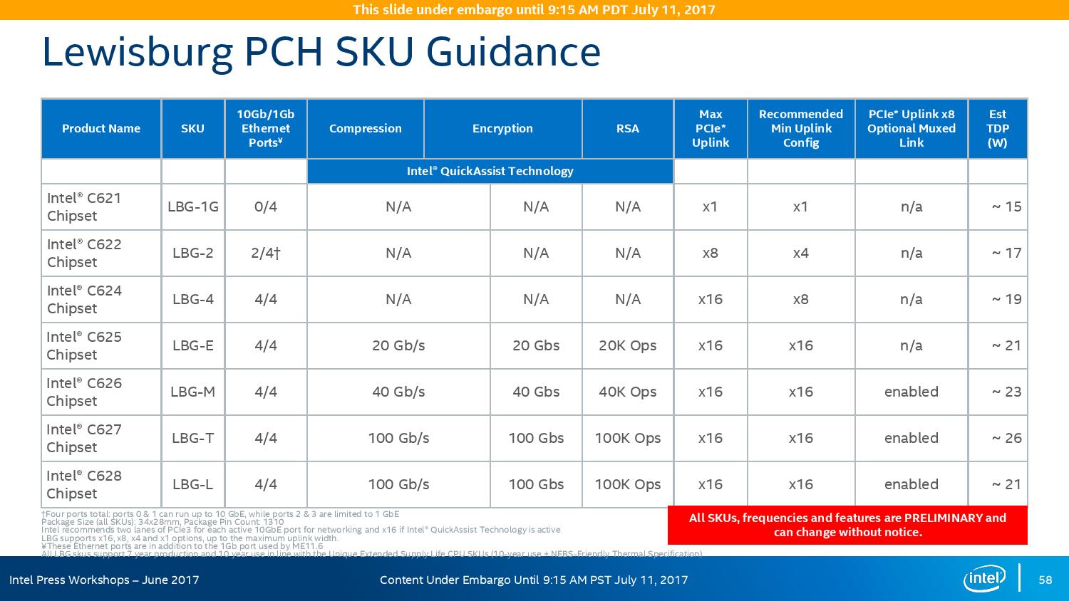
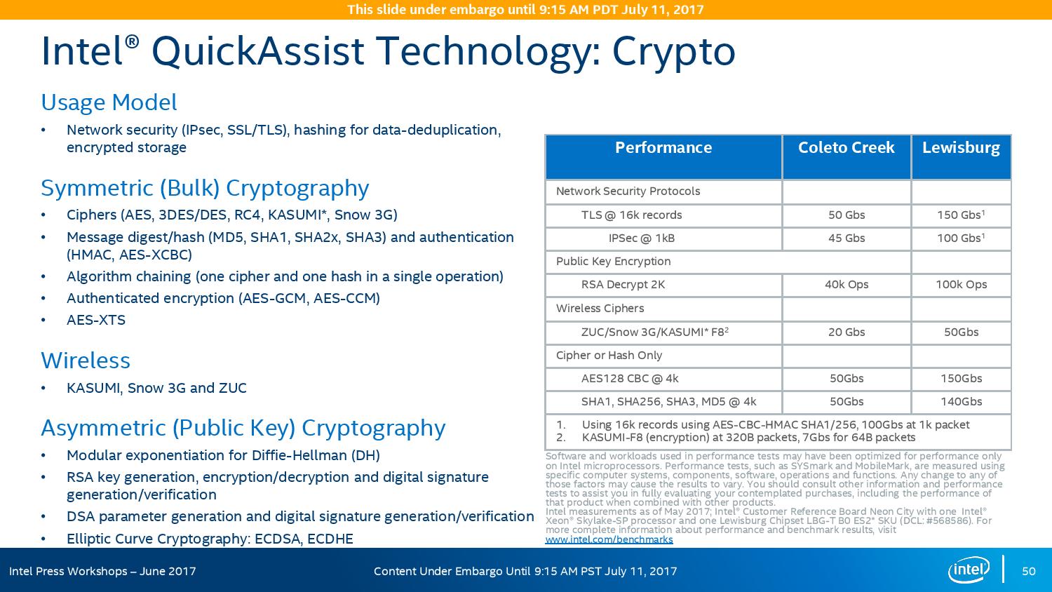
On the cryptography side, Intel has previously sold add-in PCIe cards for QuickAssist, but is now moving it onto the systems directly. By adding it into the chipset, it can be paired with the Ethernet traffic and done in-situ, and specifically Intel points to bulk cryptography (150 Gb/s AES256/SHA256), Public Key Encryption (100k ops of RSA2048) and compression (100+ Gb/s deflate).
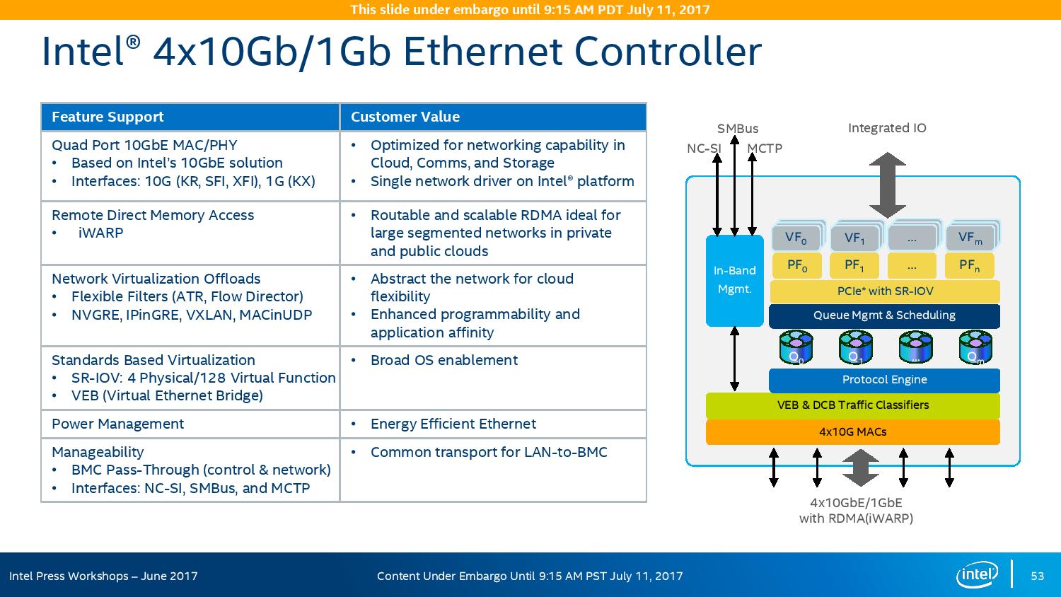
With the GbE, Intel has designed this to be paired with the X722 PHY, and supports network virtualization, traffic shaping, and supports Intel’s Data Plane Development Kit for advanced packet forwarding.
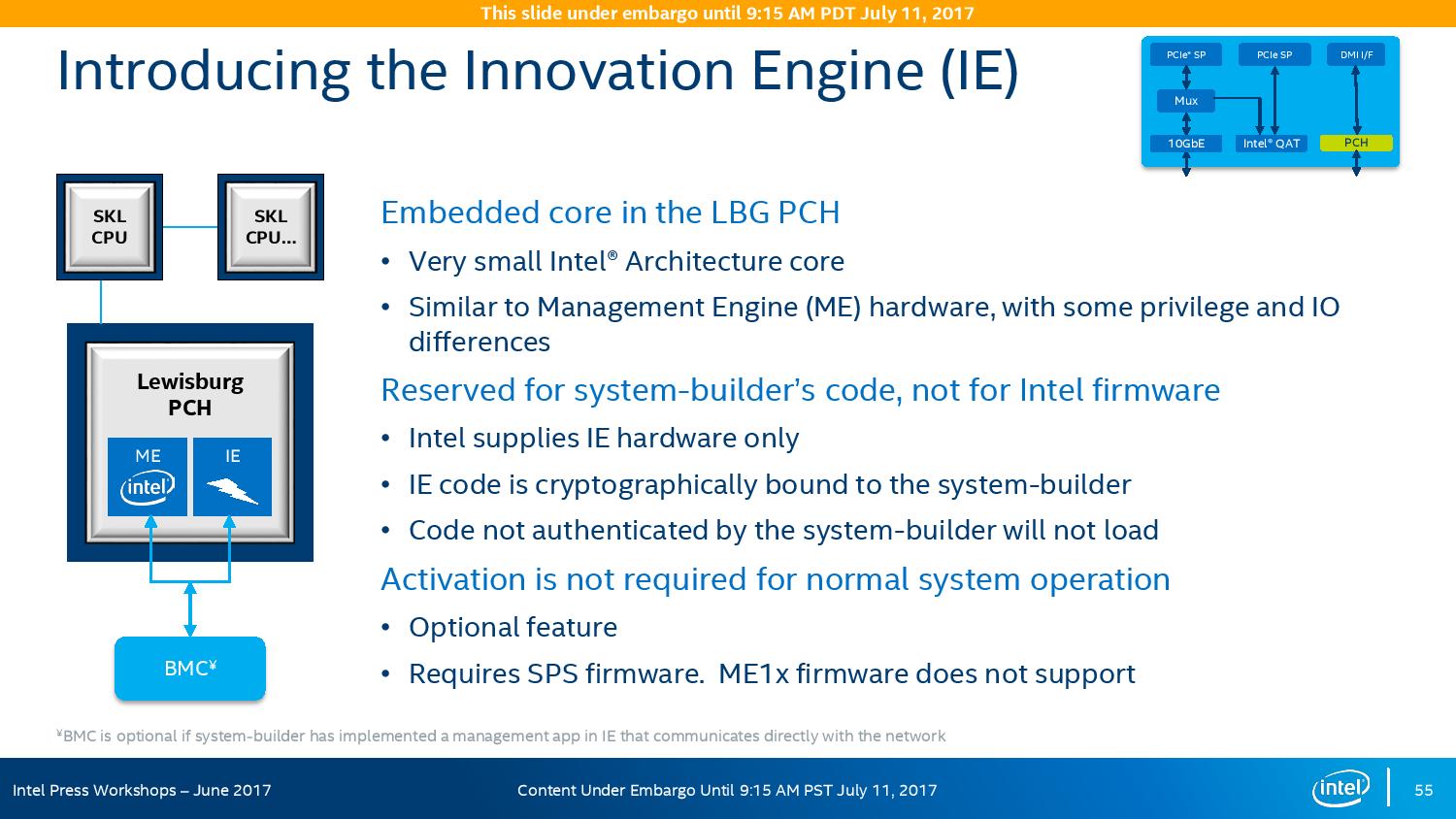
The chipset will also include a new feature called Intel’s Innovation Engine, giving a small embedded core into the PCH which mirrors Intel’s Management Engine but is designed for system-builders and integrators. This allows specialist firmware to manage some of the capabilities of the system on top of Intel’s ME, and is essentially an Intel Quark x86 core with 1.4MB SRAM.
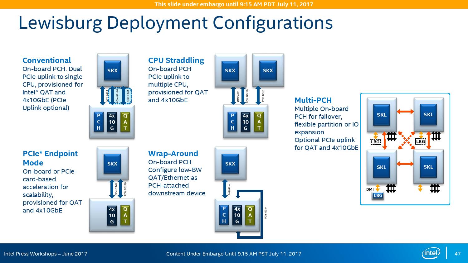
The chipsets are also designed to be supported between different CPUs within the same multi-processor system, or for a system to support multiple chipsets at once as needed.


219 Comments
View All Comments
PixyMisa - Tuesday, July 11, 2017 - link
No, the pricing is correct. The 1P CPUs really are half the price of a single 2P CPU.msroadkill612 - Wednesday, July 12, 2017 - link
Seems to me, the simplest explanation of something complex, is to list what it will not do, which they will not do :(.Can i run a 1p Epyc in a 2p mobo e.g., please?
PixyMisa - Thursday, July 13, 2017 - link
Short answer is no. It might boot, but only half the slots, memory, SATA and so on will be available. Two 1P CPUs won't talk to each other.A 2P Epyc will work in a 1P board though.
cekim - Tuesday, July 11, 2017 - link
One glaring bug/feature of AMD's segmentation relative to Intel's is the utter and obvious crippling of clock speeds for all but the absolute top SKUs. Fewer cores should be able to make use of higher clocks within the same TDP envelope. As a result Intel is objectively offering more and better fits up and down the sweep of cores vs clocks vs price spectrum.So, the bottom line is AMD is saying that you will have to buy the top-end, 4S SKU to get the top GHz for those applications in your mix that won't benefit from 16,18,32,128 cores.
I say all of this as someone who desperately wants EPYC to shake things up and force Intel to remove the sand-bags. I know I'm in a small, but non-zero market of users who can make use of dozens of cores, but still need 8 or fewer cores to perform on par with desktop parts for that purpose.
KAlmquist - Wednesday, July 12, 2017 - link
One possibility is that they have only a small percentage of the chips currently being produced bin well enough to be used in the highest clocking SKU's, so they are saving those chips for the most expensive offerings. Admittedly, that depends on what they are seeing coming off the production line. If they have a fair number of chips where with two very good cores, and two not so good, then it would make sense to offer a high clocking 16 core EPYC using chips with two cores disabled. But if clock speed on most chips is limited due to minor registration errors (which would affect the entire chip), then a chip with only two really good cores would require two localized defects in two separate cores, in addition to very good registration to get the two good cores. The combination might be too rare to justify a separate SKU.I would expect Global Foundries to continue to tweak its process to get better yields. In that case, more processors would end up in the highest bin, and AMD might decide to launch a higher clock speed 16 and 8 core EPYC processors, mostly using chips which bin well enough that they could have been used for the 32 core EPYC 7601.
alpha754293 - Tuesday, July 11, 2017 - link
Why does the Intel Xeon 6142 cost LESS than the 6142M? (e.g. per the table above, 6142 is shown with a price of $5946 while the 6142M costs $2949)ca197 - Tuesday, July 11, 2017 - link
I assume that is the wrong way round on the list. I have seen it reported the other way round on other sites.Ian Cutress - Tuesday, July 11, 2017 - link
You're correct. I've updated the piece, was a misread error from Intel's tables.coder543 - Tuesday, July 11, 2017 - link
On page 6, it says that Epyc only has 64 PCIe lanes (available), but that's not correct. There are 128 PCIe lanes per chip. In a 1P configuration, that's 128 PCIe lanes available. On a 2P configuration, 64 PCIe lanes from each chip are used to connect to the other chip, leaving 64 + 64 = 128 PCIe lanes still available.This is a significant advantage.
Ian Cutress - Tuesday, July 11, 2017 - link
You misread that table. It's quoting per-CPU when in a 2P configuration.