AMD Zen Microarchiture Part 2: Extracting Instruction-Level Parallelism
by Ian Cutress on August 23, 2016 8:45 PM EST- Posted in
- CPUs
- AMD
- x86
- Zen
- Microarchitecture
The High-Level Zen Overview
AMD is keen to stress that the Zen project had three main goals: core, cache and power. The power aspect of the design is one that was very aggressive – not in the sense of aiming for a mobile-first design, but efficiency at the higher performance levels was key in order to be competitive again. It is worth noting that AMD did not mention ‘die size’ in any of the three main goals, which is usually a requirement as well. Arguably you can make a massive core design to run at high performance and low latency, but it comes at the expense of die size which makes the cost of such a design from a product standpoint less economical (if AMD had to rely on 500mm2 die designs in consumer at 14nm, they would be priced way too high). Nevertheless, power was the main concern rather than pure performance or function, which have been typical AMD targets in the past. The shifting of the goal posts was part of the process to creating Zen.
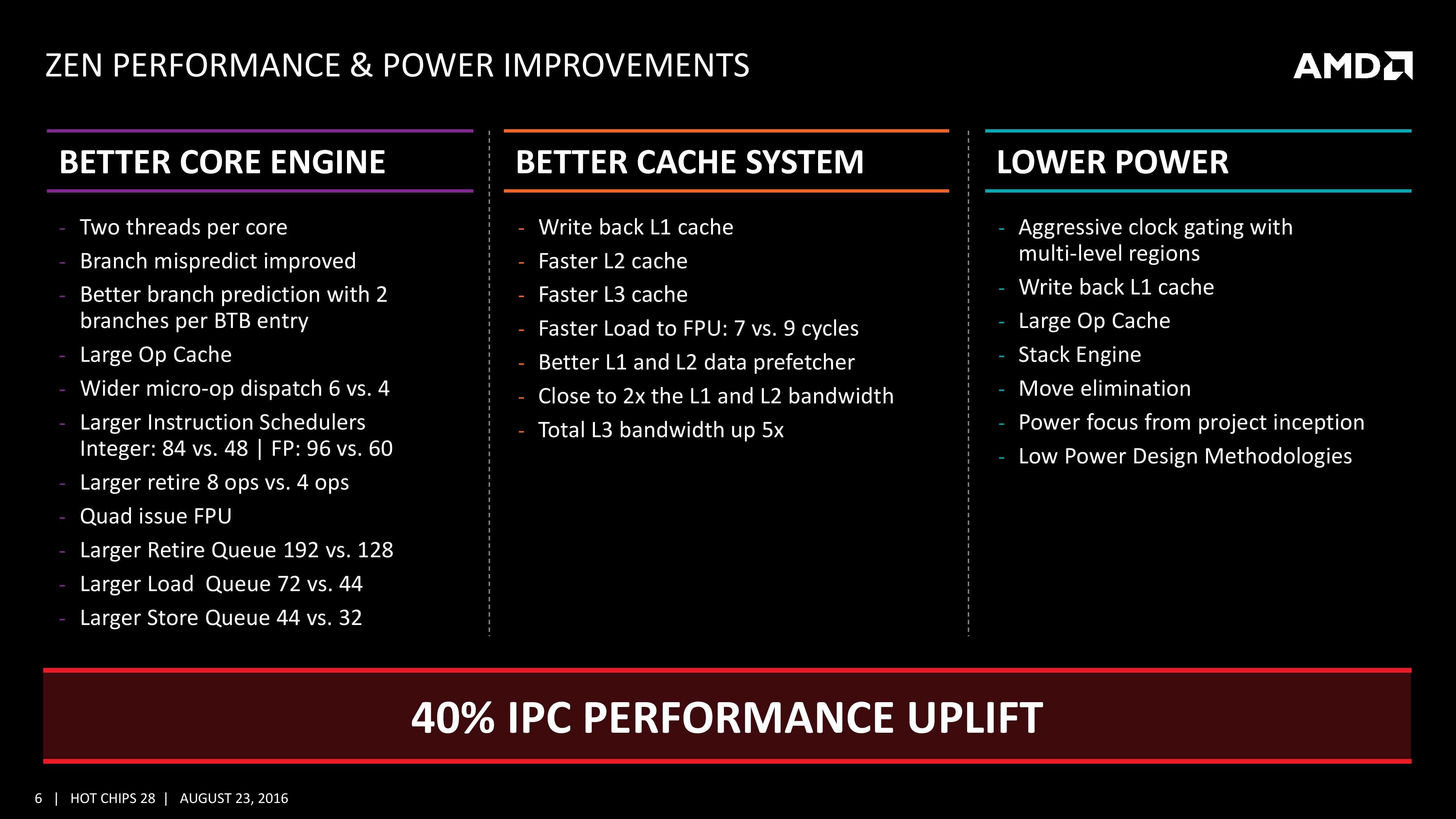
This slide contains a number of features we will hit on later in this piece but covers a number of main topics which come under those main three goals of core, cache and power.
For the core, having bigger and wider everything was to be expected, however maintaining a low latency can be difficult. Features such as the micro-op cache help most instruction streams improve in performance and bypass parts of potentially long-cycle repetitive operations, but also the larger dispatch, larger retire, larger schedulers and better branch prediction means that higher throughput can be maintained longer and in the fastest order possible. Add in dual threads and the applicability of keeping the functional units occupied with full queues also improves multi-threaded performance.
For the caches, having a faster prefetch and better algorithms ensures the data is ready when each of the caches when a thread needs it. Aiming for faster caches was AMD’s target, and while they are not disclosing latencies or bandwidth at this time, we are being told that L1/L2 bandwidth is doubled with L3 up to 5x.
For the power, AMD has taken what it learned with Carrizo and moved it forward. This involves more aggressive monitoring of critical paths around the core, and better control of the frequency and power in various regions of the silicon. Zen will have more clock regions (it seems various parts of the back-end and front-end can be gated as needed) with features that help improve power efficiency, such as the micro-op cache, the Stack Engine (dedicated low power address manipulation unit) and Move elimination (low-power method for register adjustment - pointers to registers are adjusted rather than going through the high-power scheduler).
The Big Core Diagram
We saw this diagram last week, but now we get updates on some of the bigger features AMD wants to promote:
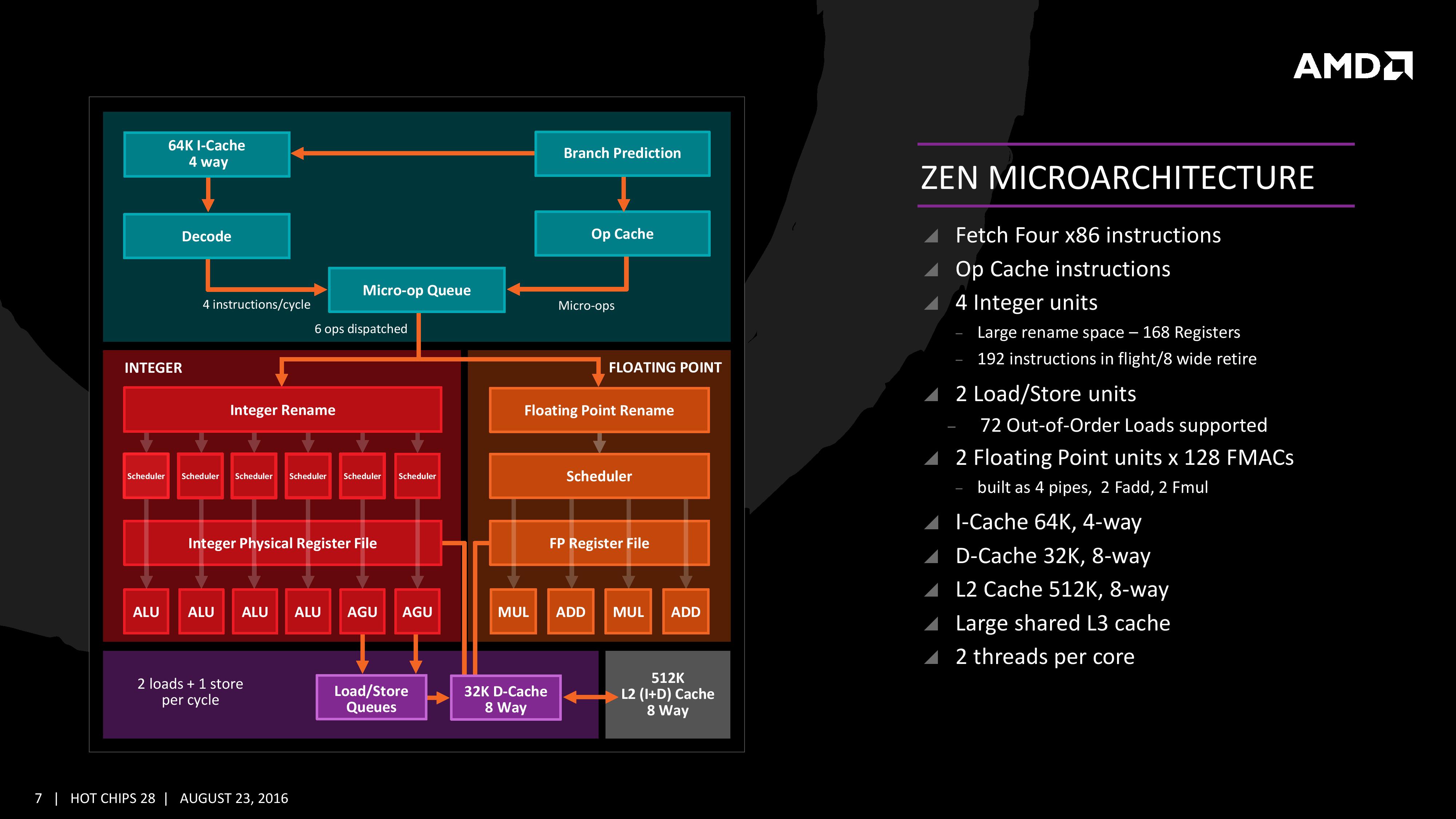
The improved branch predictor allows for 2 branches per Branch Target Buffer (BTB), but in the event of tagged instructions will filter through the micro-op cache. On the other side, the decoder can dispatch 4 instructions per cycle however some of those instructions can be fused into the micro-op queue. Fused instructions still come out of the queue as two micro-ops, but take up less buffer space as a result.
As mentioned earlier, the INT and FP pipes and schedulers are separated, but the INT rename space is 168 registers wide, which feeds into 6x14 scheduling queues. The FP employs as 160 entry register file, and both the FP and INT sections feed into a 192-entry retire queue. The retire queue can operate at 8 instructions per cycle, moving up from 4/cycle in previous AMD microarchitectures.
The load/store units are improved, supporting a 72 out-of-order loads, similar to Skylake. We’ll discuss this a bit later. On the FP side there are four pipes (compared to three in previous designs) which support combined 128-bit FMAC instructions. These cannot be combined for one 256-bit AVX2, but can be scheduled for AVX2 over two instructions.


106 Comments
View All Comments
bcronce - Tuesday, August 23, 2016 - link
Exclusive L3 cache makes better use of space, but requires snooping other core's L2 caches for data. If the L3 cache has all of the data all of the L2 cache has, then you only need to check one place.This is important when you're trying to synchronize threads since locks are shared memory locations that each core is attempting to read and update. Common types of thread safe data-structures can take some pretty big performance scaling hits. Of course you can work around this in your data-structure.
One research paper that I read showed exclusive caches having twice the latency of inclusive when snooping was required. If your data-structure has a scaling that works well up to 16 cores on Intel's inclusive cache, it may cap out around 8 cores on AMD's exclusive, thanks to Amdahl's law.
Cache snooping gets slower as more cores are added. Gotta check them all.
deltaFx2 - Tuesday, August 23, 2016 - link
@bconce: Except that Intel doesn't do strictly inclusive caches either. Intel's caches are neither-inclusive-nor-exclusive (afaik), in which data is inserted into both L2 and L3, but evicted independently. So you have to check L2 and L3 independently, same as the exclusive cache. Strictly-inclusive caches have many bad properties, a few that come to mind immediately (1) False evictions of lines: If a block constantly hits in L2, the LRU in L3 is not updated. If the block then becomes the oldest in L3 and is evicted, it must be evicted in L2 as well, resulting in a miss all the way to memory (2) Associativity of the L3 cache must be at least the sum of the associativity of the L2 caches hanging off it, otherwise it will constrain the associativity of the L2 caches. Hence neither-inclusive-nor-exclusive, or strictly exclusive.Exclusive caches are harder to build, true, because you have to manage exclusivity. That doesn't explain Ian's comment about them being less efficient.
68k - Wednesday, August 24, 2016 - link
The Intel manual state that"The shared L3 cache is writeback and inclusive, such that a cache line that exists in either L1 data cache, L1 instruction cache, unified L2 cache also exists in L3."
That is, the L3-cache is strictly inclusive with anything stored in the core local L2/L1-caches. So it is enough to check L3 to see whether the cache-line is in use by any other core sharing the L3.
bcronce - Wednesday, August 24, 2016 - link
@68kThanks for looking it up. I only remembered Intel talking talking about this years ago when they made the design decision in order to minimize latency. Certain operations are extremely latency sensitive, like thread synchronizations.
The strange thing is AMD is pushing for so many cores, but then chooses a cache design that makes sharing data more expensive. What they did gain is exclusive caches tend to have more bandwidth and are great for independent threads with little sharing. It's a trade off. Nothing is free, pros and cons everywhere.
deltaFx2 - Wednesday, August 24, 2016 - link
@68k,@bcronce: I guess I haven't looked up Intel's latest and greatest cache organization :) I do recall though that Neither-incl-nor-exclusive was their scheme for quite a while, probably until Sandy Bridge. Perhaps that explains why their L2 cache went from 8-way to 4-way in SkyLake; the extra associativity cannot be effectively utilized with strict inclusion as you keep adding more cores (a single set in L3 maps to a unique set in L2. If you have 16 way L3, only 16 lines that map to that set in L3 can reside in the L2s. Obviously, multiple L3 sets map to the same L2 set, so this is somewhat mitigated, but it is a glass-jaw).The nice thing about Intel's organization is that it's a monolithic L3 with variable latency to slices, as opposed to AMD's distributed L3. That probably is what adds the latency (if it does) on cache-to-cache transfers, not the inclusive-vs-exclusive, or the inclusive cache acting as a probe filter. You could just as easily add a separate probe filter to avoid unnecessary coherence lookups. Would you point me to that paper you quoted earlier? I have a hard time believing that the problem is the exclusive cache itself, and not the organization of the cache. Anyway, I don't know enough about AMD's design to comment, so I'll leave it at that. Thanks!
intangir - Wednesday, August 24, 2016 - link
As far as I know, since Nehalem Intel's L3 caches have been fully inclusive of L1+L2, but the L1 and L2 caches are neither inclusive nor exclusive with respect to each other.Ryan Smith - Tuesday, August 23, 2016 - link
Right you are. That's a typo on our end, and in the deep dive section on cache you can see why it's exclusive. As for the first page, I've corrected the typo.looncraz - Wednesday, August 24, 2016 - link
Zen's L3 is "mostly exclusive." This changes things up a bit - it isn't a pure victim cache and will probably contain data used between multiple cores. The first access will be slower as the data is snooped from another core's L2, but then that data will be mirrored in the L3. The coherent data fabric which links multiple core complexes adds a whole new level of complexity for sharing data between cores, but I suspect a mechanism exists to synchronize global data between the L3 caches, so global data will have a copy in each L3 and actions on global data will incur a latency penalty, but nothing compared to snooping L2s across multiple core complexes.NikosD - Wednesday, August 24, 2016 - link
It seems that AMD did its job right this time.Most of the CPU features are in between Broadwell and Skylake architectures and this is extremely important and fast, with the exception of AVX/AVX2 instructions that are executed in 128bit chunks instead of 256bit.
Of course we have to wait and see latencies and throughput of the rest of arithmetic instructions, but all these are just details.
I think with Zen we will all owe a lot to AMD like the older days of 64bit CPUs and OS.
This time the revolution will be the affordable true 8 core/ 16 thread CPU with no GPU inside for the first time in desktop.
The key point here is price, in order to be affordable. Not like High-End Desktop systems of Intel.
That move will force Intel to accept the fact that we, as customers, want 8 cores in our CPUs like 64bit CPUs and OS back in the past that Intel offered only with Itanium.
All in all, AMD could possibly hold in its hands a true winner, from laptops to servers that brings us memories of AMD Athlon and Opteron CPUs.
Well done AMD!
Michael Bay - Wednesday, August 24, 2016 - link
Do we, though? General purpose software like word processors and such is literally indistinguishable on 2 and 4 cores, and a lot of things on content creation side are already accelerated by GPU.There are games of course, but CPU stopped being a bottleneck there long time ago.