AMD Zen Microarchiture Part 2: Extracting Instruction-Level Parallelism
by Ian Cutress on August 23, 2016 8:45 PM EST- Posted in
- CPUs
- AMD
- x86
- Zen
- Microarchitecture
Execution, Load/Store, INT and FP Scheduling
The execution of micro-ops get filters into the Integer (INT) and Floating Point (FP) parts of the core, which each have different pipes and execution ports. First up is the Integer pipe which affords a 168-entry register file which forwards into four arithmetic logic units and two address generation units. This allows the core to schedule six micro-ops/cycle, and each execution port has its own 14-entry schedule queue.
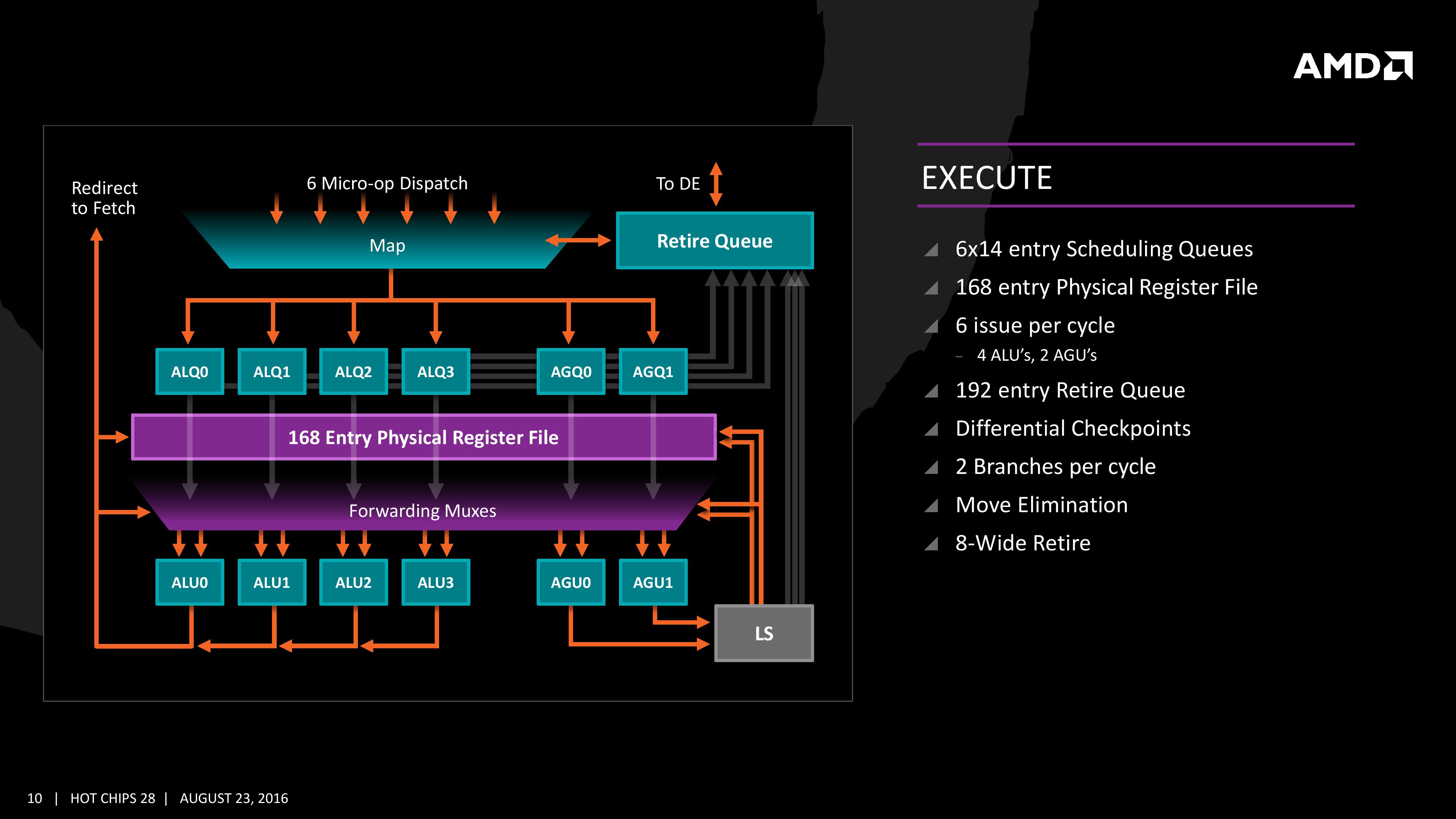
The INT unit can work on two branches per cycle, but it should be noted that not all the ALUs are equal. Only two ALUs are capable of branches, one of the ALUs can perform IMUL operations (signed multiply), and only one can do CRC operations. There are other limitations as well, but broadly we are told that the ALUs are symmetric except for a few focused operations. Exactly what operations will be disclosed closer to the launch date.
The INT pipe will keep track of branching instructions with differential checkpoints, to cut down on storing redundant data between branches (saves queue entries and power), but can also perform Move Elimination. This is where a simple mov command between two registers occurs – instead of inflicting a high energy loop around the core to physically move the single instruction, the core adjusts the pointers to the registers instead and essentially applies a new mapping table, which is a lower power operation.
Both INT and FP units have direct access to the retire queue, which is 192-entry and can retire 8 instructions per cycle. In some previous x86 CPU designs, the retire unit was a limiting factor for extracting peak performance, and so having it retire quicker than dispatch should keep the queue relatively empty and not near the limit.
The Load/Store Units are accessible from both AGUs simultaneously, and will support 72 out-of-order loads. Overall, as mentioned before, the core can perform two 16B loads (2x128-bit) and one 16B store per cycle, with the latter relying on a 44-entry Store queue. The TLB buffer for the L2 cache for already decoded addresses is two level here, with the L1 TLB supporting 64-entry at all page sizes and the L2 TLB going for 1.5K-entry with no 1G pages. The TLB and data pipes are split in this design, which relies on tags to determine if the data is in the cache or to start the data prefetch earlier in the pipeline.
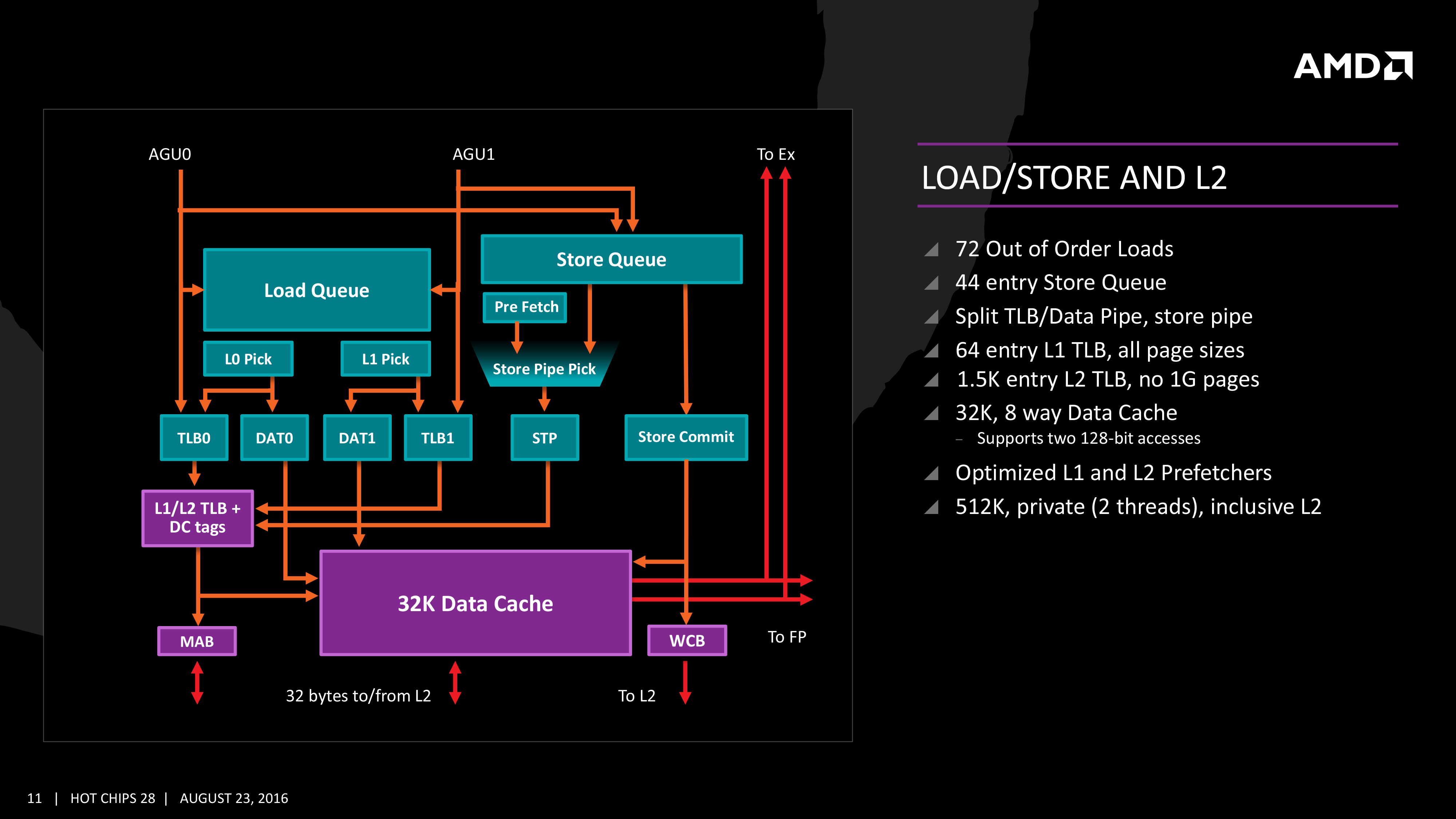
The data cache here also has direct access to the main L2 cache at 32 Bytes/cycle, with the 512 KB 8-way L2 cache being private to the core and inclusive. When data resides back in L1 it can be processed back to either the INT or the FP pipes as required.
Moving onto the floating point part of the core, and the first thing to notice is that there are two scheduling queues here. These are listed as ‘schedulable’ and ‘non-schedulable’ queues with lower power operation when certain micro-ops are in play, but also allows the backup queue to sort out parts of the dispatch in advance via the LDCVT. The register file is 160 entry, with direct FP to INT transfers as required, as well as supporting accelerated recovery on flushes (when data is written to a cache further back in the hierarchy to make room).
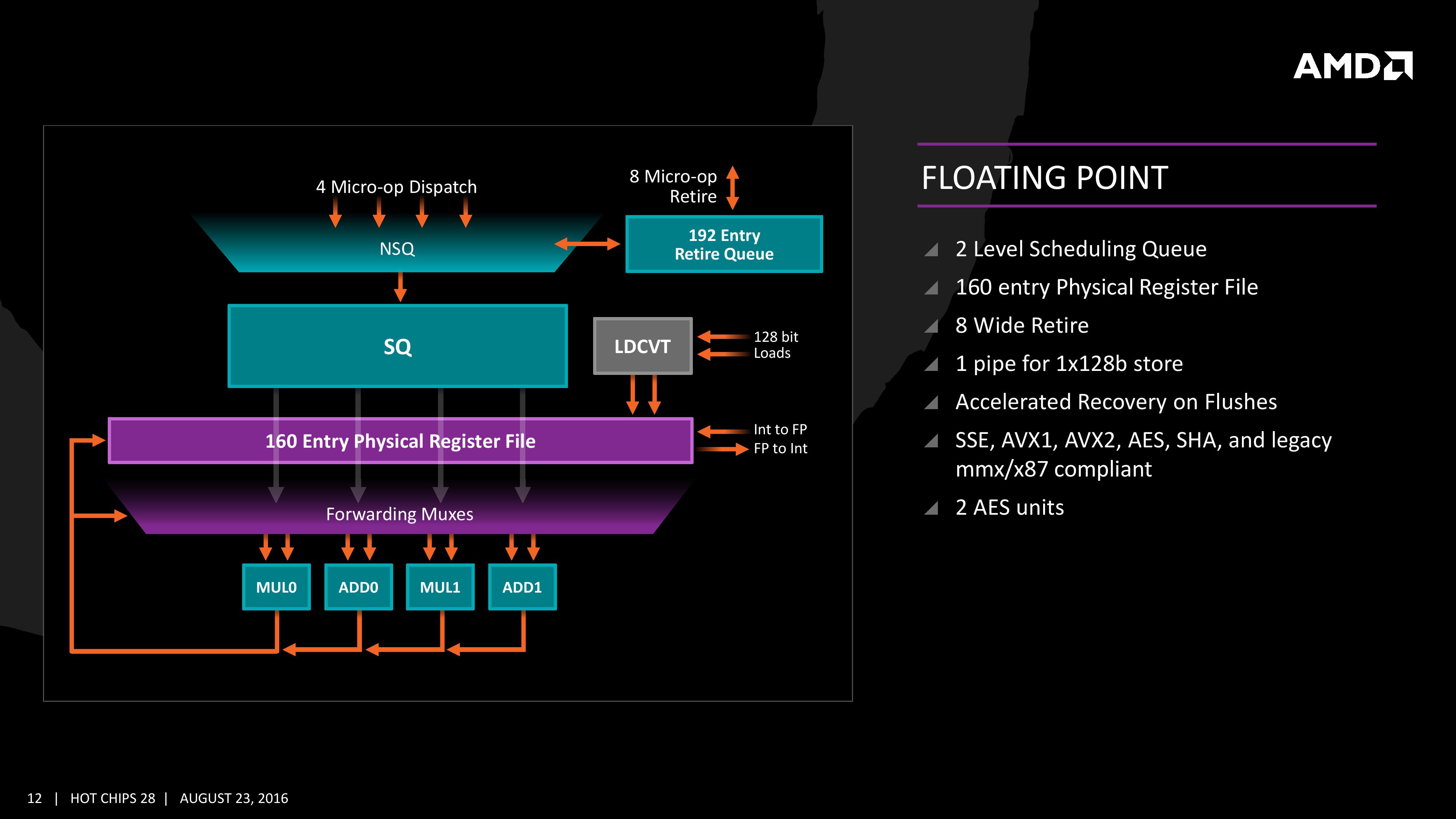
The FP Unit uses four pipes rather than three on Excavator, and we are told that the latency in Zen is reduced as well for operations (though more information on this will come at a later date). We have two MUL and two ADD in the FP unit, capable of joining to form two 128-bit FMACs, but not one 256-bit AVX. In order to do AVX, the unit will split the operations accordingly. On the counter side each core will have 2 AES units for cryptography as well as decode support for SSE, AVX1/2, SHA and legacy mmx/x87 compliant code.


106 Comments
View All Comments
tipoo - Wednesday, August 31, 2016 - link
Bulldozers engineering samples were 2.5GHz and that shipped stupid high clocked. Zen ESs being 3GHz doesn't worry me.Cooe - Thursday, May 6, 2021 - link
Holy CRAP did history ever make you look like an absolute freaking idiot! xDextide - Monday, August 29, 2016 - link
Well, they have already shown an 8-core Zen running at full load at 3Ghz with their regular OEM heatsink/fans, and those are rated at 125W TDP max, so we do already know that's possible.defter - Wednesday, August 24, 2016 - link
It's 40% IPC improvement, not 40% overall improvement. If you improve IPC by 40% and achieve 85% of the clock speed, the total improvement will be only 20%.Since AMD hasn't talked about clock speed we can assume that it will be lower than Bulldozer.
euskalzabe - Wednesday, August 24, 2016 - link
Let me fix that for you: "Since AMD hasn't talked about clock speed we can assume..." absolutely nothing and can only wait until the final product is released.retrospooty - Wednesday, August 24, 2016 - link
Actually he is right and probably understating it. If AMD says it qill have 40% IPC improvement, it is probably not true, or true only in a few select benchmarks. If AMD left out the clockspeed it is almost definitely going to lower. AMD has zero credibility with pre-release performance claims. Nothing AMD says can be takes at its word until retail units (not engineering samples) are independently tested.Azix - Wednesday, August 24, 2016 - link
why the flying fork would the clock speed be lower? I hope you dont mean lower than they have shown, that would make no sense.Bulldozer engineering samples were maybe 2.5Ghz or 3Ghz. Additionally, talking about actual clock speeds would be to give away sku information. How they plan to structure the product line etc.
Outlander_04 - Thursday, August 25, 2016 - link
Both intel Broadwell-e and Zen were at 3 Ghz for the comparison .Broadwell-e maxes out at 3.6 Ghz , but most models are at 3.2 Ghz .
Dont let your prejudices cause you to jump to conclusions.
Zen could easily be released running at higher clock rates
silverblue - Wednesday, August 24, 2016 - link
Imagine for a second that Zen was clocked like the FX-8320E, that is a 3.2GHz base with 4.0GHz boost. Would a 40 to 50% average IPC boost make Zen competitive?For all we know, Zen could be conservatively clocked, paving the way for Zen+ with moderate tweaks and increased clocks; a bit like Piledriver vs. Bulldozer, as opposed to Phenom II vs. Phenom.
looncraz - Wednesday, August 24, 2016 - link
Zen will clock very close to 4Ghz out of the box - AMD kept most of the speed-demon elements of Bulldozer, such as the long pipelines. They also used dedicated, simple, schedulers - which is where frequency limits are frequently found... and they also put the L3 cache on a different clock bus, meaning it might operate at a different frequency from the cores... again.The engineering samples are always clocked low, so if they are running at 3Ghz for a demo, then they will be able to achieve at least 3.4~3.6Ghz, with 4Ghz boost clocks on eight-core CPUs. Quad core units will obviously go higher, still. That is why half the cores still has 70% of the power draw - it's operating higher up the frequency curve. 3.8Ghz base, 4.2Ghz boost for the top quad core SKU seems very likely given what is known.