AMD Zen Microarchiture Part 2: Extracting Instruction-Level Parallelism
by Ian Cutress on August 23, 2016 8:45 PM EST- Posted in
- CPUs
- AMD
- x86
- Zen
- Microarchitecture
Execution, Load/Store, INT and FP Scheduling
The execution of micro-ops get filters into the Integer (INT) and Floating Point (FP) parts of the core, which each have different pipes and execution ports. First up is the Integer pipe which affords a 168-entry register file which forwards into four arithmetic logic units and two address generation units. This allows the core to schedule six micro-ops/cycle, and each execution port has its own 14-entry schedule queue.
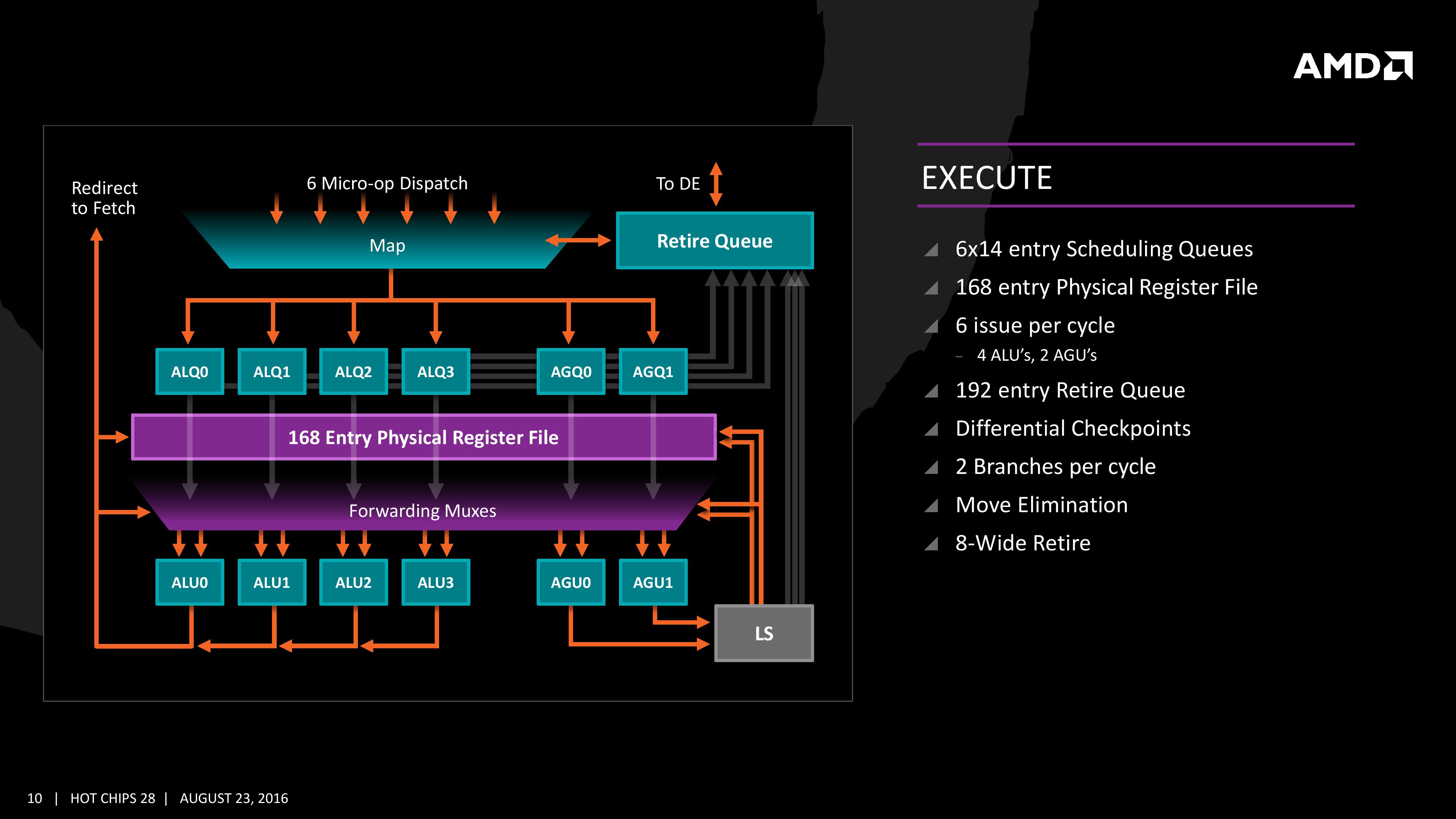
The INT unit can work on two branches per cycle, but it should be noted that not all the ALUs are equal. Only two ALUs are capable of branches, one of the ALUs can perform IMUL operations (signed multiply), and only one can do CRC operations. There are other limitations as well, but broadly we are told that the ALUs are symmetric except for a few focused operations. Exactly what operations will be disclosed closer to the launch date.
The INT pipe will keep track of branching instructions with differential checkpoints, to cut down on storing redundant data between branches (saves queue entries and power), but can also perform Move Elimination. This is where a simple mov command between two registers occurs – instead of inflicting a high energy loop around the core to physically move the single instruction, the core adjusts the pointers to the registers instead and essentially applies a new mapping table, which is a lower power operation.
Both INT and FP units have direct access to the retire queue, which is 192-entry and can retire 8 instructions per cycle. In some previous x86 CPU designs, the retire unit was a limiting factor for extracting peak performance, and so having it retire quicker than dispatch should keep the queue relatively empty and not near the limit.
The Load/Store Units are accessible from both AGUs simultaneously, and will support 72 out-of-order loads. Overall, as mentioned before, the core can perform two 16B loads (2x128-bit) and one 16B store per cycle, with the latter relying on a 44-entry Store queue. The TLB buffer for the L2 cache for already decoded addresses is two level here, with the L1 TLB supporting 64-entry at all page sizes and the L2 TLB going for 1.5K-entry with no 1G pages. The TLB and data pipes are split in this design, which relies on tags to determine if the data is in the cache or to start the data prefetch earlier in the pipeline.
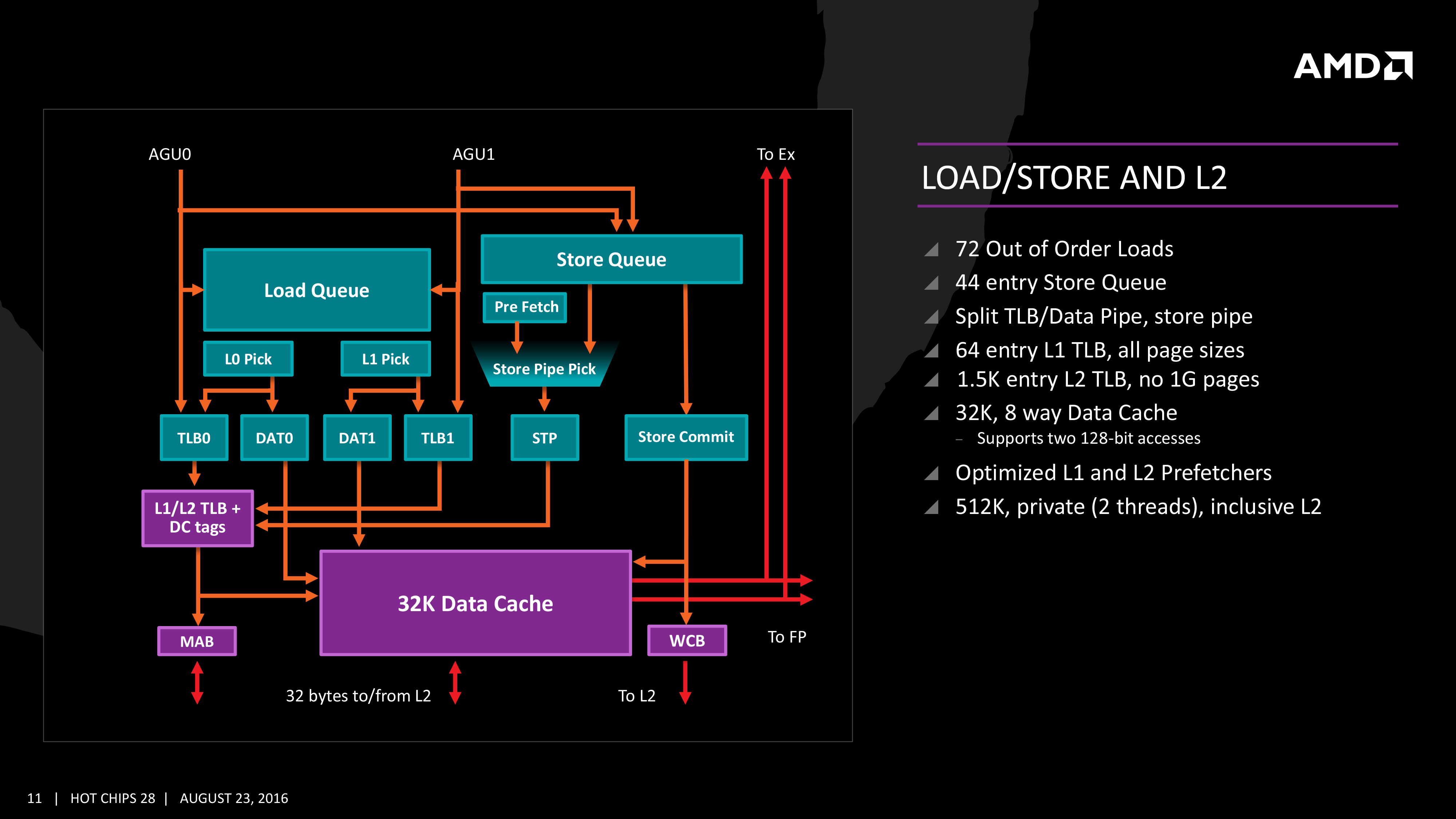
The data cache here also has direct access to the main L2 cache at 32 Bytes/cycle, with the 512 KB 8-way L2 cache being private to the core and inclusive. When data resides back in L1 it can be processed back to either the INT or the FP pipes as required.
Moving onto the floating point part of the core, and the first thing to notice is that there are two scheduling queues here. These are listed as ‘schedulable’ and ‘non-schedulable’ queues with lower power operation when certain micro-ops are in play, but also allows the backup queue to sort out parts of the dispatch in advance via the LDCVT. The register file is 160 entry, with direct FP to INT transfers as required, as well as supporting accelerated recovery on flushes (when data is written to a cache further back in the hierarchy to make room).
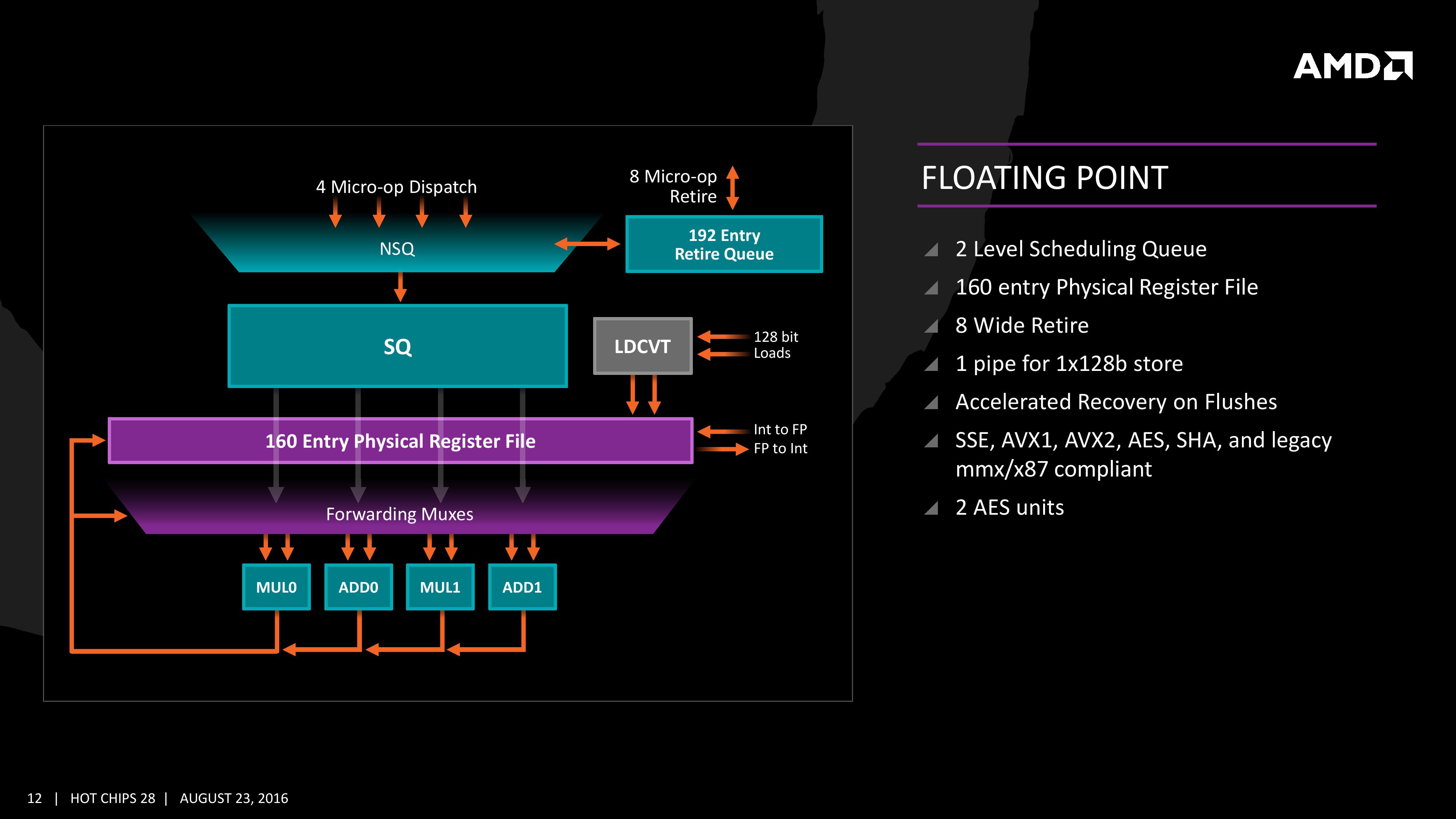
The FP Unit uses four pipes rather than three on Excavator, and we are told that the latency in Zen is reduced as well for operations (though more information on this will come at a later date). We have two MUL and two ADD in the FP unit, capable of joining to form two 128-bit FMACs, but not one 256-bit AVX. In order to do AVX, the unit will split the operations accordingly. On the counter side each core will have 2 AES units for cryptography as well as decode support for SSE, AVX1/2, SHA and legacy mmx/x87 compliant code.


106 Comments
View All Comments
extide - Monday, August 29, 2016 - link
No,k dude, it's not the same 4 ALU's, it's 4 ALU's per core. 2 threads a core, so 2 ALU's/thread, up to 16 threads, or 4 ALU's /thread up to 8 threads, but I would think it would be hard for a single thread to use 4 ALU's, so having 2 threads per 4 ALU seems fine, plus all the INT execution resources.Outlander_04 - Thursday, August 25, 2016 - link
40% improvement is not over Bulldozer but over Excavator which is already 20% or more ahead of Bulldozerlooncraz - Wednesday, August 24, 2016 - link
Highly scalar code or vector code will exceed 40% easily. The core execution resources relative to that execution is 75% to 100% greater. That will only translate to 50~60% performance improvement for said code, but a larger impact than the overall 40% improvement.The cache system, schedulers, issue width, AGUs, L/S, and other factors come more into play in the more common code paths, which reduces the maximum potential benefit derived from the additional execution resources.
However, multi-threaded performance should be HIGHER, not lower. Excavator had relatively poor MT scaling, Zen will be worlds better. Add SMT to the mix - and AMD's solution looks nearly exactly as I anticipated - and you have another 20% or so better SMT scaling.
It is easily conceivable, given what we now know, that AMD has met Haswell's average IPC outside of wider AVX workloads, and exceeded it in certain areas with heavy mixed compute (floating and integer concurrently). It is also now conceivable that AMD's first SMT implementation will be better than Intel's Sandy Bridge era Hyper-Threading. I didn't expect that at all, but the core flexibility is far ahead of Intel's flexibility - and that is largely what determines SMT performance in Zen's design.
Finally, <3Ghz @ 200W is way worse than the currently known figures for their 8C parts. They have 3.2Ghz boost clocks and just 95W TDP. It is expected that the clocks will increase, particularly for the quad core, 65W, parts.
You may not realize this, but these numbers put AMD slightly ahead of Intel in perf/W on 14nm.
niva - Wednesday, August 24, 2016 - link
So are you telling me my Phenom 2 black edition rig might be getting a worthy upgrade?I'm with you, but I don't trust these benchmarks, wait until the retail CPU samples are out then we can decide.
looncraz - Wednesday, August 24, 2016 - link
I'm saying you'll be able to match that level of performance with a Dual core Zen CPU w/ SMT... if AMD were actually to make one (doubtful).I do expect AMD to release triple core CPUs again, though, but possibly not right away.
Myrandex - Thursday, August 25, 2016 - link
Yay finally I've been holding onto my Phenom II as well and this might be it! :)Bulat Ziganshin - Thursday, August 25, 2016 - link
For vector code - they added 4'th ALU, it's almost nothing (Skylake added 4th scalar ALU and got laughable +3% IPC).For scalar code - they advertize +40% IPC. I'm pretty sure that they advertize the best part of perfromance, not the average one. It's ADVERTIZEMENT, after all.
Now, it's easy to analyze Zen as Carrizo+. M/t performance shouldn't change much since it's still 4-wide core (which was called module in Carrizo). S/t performance should improve much more since it changed from 2 alu to 4 alu. Overall, the core looks like Skylake, but it's not enough to put a lot of resources - they need to be carefully placed. Intel gone a long way optimizing their CPUs, and AMD have to repeat that. If you think that AMD can make Skylake-speed CPU in 2 years, then ask yourself - why Intel hasn't done the same in 2008 or so? Why IBM, having WIDER cpu, still slower than Intel in s/t tests?
All we know that AMD was able to SELECT single CPU that was able to run at 3 GHz using cooler looking like one they ship with 95W cpus. Just ask yourself - why they not tried to run their cpu at the same 3.2 GHz which is stock freq. for Intel CPU? And yes, it's way more effificent than Intel CPUs can, making me highly suspicious.
In one of pictures here AMD claims that Zen has the same power usage as Carrizo, that is 28nm CPU. AFAIR Carrizo with 2 modules at ~3GHz use 35-65 Wt. Multiple it by 4, please.
> It is also now conceivable that AMD's first SMT implementation will be better than Intel's Sandy Bridge era Hyper-Threading.
Why?? Intel's first SMT implementation in Pentium4 made a few percents improvement (over s/t), second one in Nehalem give me +20% on deflate, Sandy was +40%, and Haswell is +50%. Why you think that FIRST AMD attempt on SMT will be better than Pentium4?
Overall, i think that m/t perfromance of Zen is more predictable - it's Carrizo with some improvements, but still 4-wide, so i expect usual 10-20% generation-to-generation improvement.
For s/t, it less predictable, but i'm sure that it's impossible to beat Intel in single step, and AMD already advertized +40%, which i'm sure is about s/t perfromance.
looncraz - Thursday, August 25, 2016 - link
"For vector code - they added 4'th ALU, it's almost nothing (Skylake added 4th scalar ALU and got laughable +3% IPC)."Well, that was the average program performance increase, but the vector code itself sped up more than that.
Also, Zen's ability to leverage its resources should be better than Intel's, but its scheduler setup is really unique, so we need more details on how it will handle holes in a scheduler when its neighbor is full. Having six 14-deep schedulers is a significant part of the design that is almost completely overlooked, IMHO.
"Now, it's easy to analyze Zen as Carrizo+. M/t performance shouldn't change much since it's still 4-wide core"
Only if you are comparing a full module to a single Zen core... There were many bottlenecks in the modules that prevented full performance for multi-threading - Zen does not have that. On top, Zen has SMT, so it will have even better MT performance per core.
"Why IBM, having WIDER cpu, still slower than Intel in s/t tests?"
The width is, as you say, only a part of the equation. It's all about being able to exploit that extra width. Intel does so decently well, but has restrictions as a result of their unified scheduler. A heavy FPU load reduces integer performance, for example, due to shared ports of the scheduler. The impact of this is not easily quantifiable - it would require some very specialized testing. Zen will not have this issue thanks to dedicated schedulers.
Intel uses their unified scheduler to be able to provide results more quickly to dependent instructions. Zen, from appearances, allows each scheduler to make fetch and load requests directly, thereby nullifying what used to be an Intel advantage - and maybe even turning it into a hindrance.
"Just ask yourself - why they not tried to run their cpu at the same 3.2 GHz which is stock freq. for Intel CPU?"
Because you don't push engineering sample CPUs, and 3Ghz is the defacto industry standard speed for IPC comparison testing. Just look around, you'll find 3Ghz is the most commonly chosen frequency when doing IPC comparisons on modern CPUs. Pushing both to 3.2Ghz would not have changed anything, but a Zen engineering sample chip is worth thousands more than that Intel CPU at this time, and is not easily replaceable. If you have to run 500 more tests with it, and hand it over to other departments or teams, you probably aren't being allowed to overclock it any.
deltaFx2 - Friday, August 26, 2016 - link
The answer to the IBM question is easy. 1) IBM designed the Power8 with SMT-2 as the sweet spot. Like bulldozer, or Alpha EV6, they have execution clusters. In 2T, each cluster runs a thread, in 1T, the thread is split across these clusters, with a penalty for moving between them. Hence their 1T->2T uplift is a lot higher than intel's 1T->2T (worse baseline). (2) You're comparing different ISAs. x86 is a lot more CISC'y than POWER. x86 supports load+compute, compute+store, load+compute+store, and this is dispatched as a single uop. The same "work" in a more RISC'y machine needs 2 or 3 uops. For the same reason, an ARM core that hopes to achieve the same performance as x86 will need to dispatch more ops, or fuse more ops before dispatch.Spunjji - Saturday, August 27, 2016 - link
The CPU they tasted with is an early engineering sample. Simple answer. You write a lot to make yourself sound smart but you're exercising either clear bias or ignorance here.