AMD Zen Microarchiture Part 2: Extracting Instruction-Level Parallelism
by Ian Cutress on August 23, 2016 8:45 PM EST- Posted in
- CPUs
- AMD
- x86
- Zen
- Microarchitecture
Some Final Thoughts and Comparisons
With the Hot Chips presentation we’ve been given more information on the Zen core microarchitecture than we expected to have at this point in the Zen design/launch cycle. AMD has already stated that general availability for Zen will be in Q1, and Zen might not be the final product launch name/brand when it comes to market. However, there are still plenty of gaps in our knowledge for the hardware, and AMD has promised to reveal this information as we get closer to launch.
We discussed in our earlier piece on the Zen performance metrics given mid-week that it can be hard to interpret any anecdotal benchmark data at this point when there is so much we don’t know (or can’t confirm). With the data in this talk at Hot Chips, we can fill out a lot of information for a direct comparison chart to AMD’s last product and Intel’s current offerings.
| CPU uArch Comparison | ||||
| AMD | Intel | |||
| Zen 8C/16T 2017 |
Bulldozer 4M / 8T 2010 |
Skylake 4C / 8T 2015 |
Broadwell 8C / 16T 2014 |
|
| L1-I Size | 64KB/core | 64KB/module | 32KB/core | 32KB/core |
| L1-I Assoc | 4-way | 2-way | 8-way | 8-way |
| L1-D Size | 32KB/core | 16KB/thread | 32KB/core | 32KB/core |
| L1-D Assoc | 8-way | 4-way | 8-way | 8-way |
| L2 Size | 512KB/core | 1MB/thread | 256KB/core | 256KB/core |
| L2 Assoc | 8-way | 16-way | 4-way | 8-way |
| L3 Size | 2MB/core | 1MB/thread | >2MB/cire | 1.5-3MB/core |
| L3 Assoc | 16-way | 64-way | 16-way | 16/20-way |
| L3 Type | Victim | Victim | Write-back | Write-back |
| L0 ITLB Entry | 8 | - | - | - |
| L0 ITLB Assoc | ? | - | - | - |
| L1 ITLB Entry | 64 | 72 | 128 | 128 |
| L1 ITLB Assoc | ? | Full | 8-way | 4-way |
| L2 ITLB Entry | 512 | 512 | 1536 | 1536 |
| L2 ITLB Assoc | ? | 4-way | 12-way | 4-way |
| L1 DTLB Entry | 64 | 32 | 64 | 64 |
| L1 DTLB Assoc | ? | Full | 4-way | 4-way |
| L2 DTLB Entry | 1536 | 1024 | - | - |
| L2 DTLB Assoc | ? | 8-way | - | - |
| Decode | 4 uops/cycle | 4 Mops/cycle | 5 uops/cycle | 4 uops/cycle |
| uOp Cache Size | ? | - | 1536 | 1536 |
| uOp Cache Assoc | ? | - | 8-way | 8-way |
| uOp Queue Size | ? | - | 128 | 64 |
| Dispatch / cycle | 6 uops/cycle | 4 Mops/cycle | 6 uops/cycle | 4 uops/cycle |
| INT Registers | 168 | 160 | 180 | 168 |
| FP Registers | 160 | 96 | 168 | 168 |
| Retire Queue | 192 | 128 | 224 | 192 |
| Retire Rate | 8/cycle | 4/cycle | 8/cycle | 4/cycle |
| Load Queue | 72 | 40 | 72 | 72 |
| Store Queue | 44 | 24 | 56 | 42 |
| ALU | 4 | 2 | 4 | 4 |
| AGU | 2 | 2 | 2+2 | 2+2 |
| FMAC | 2x128-bit | 2x128-bit 2x MMX 128-bit |
2x256-bit | 2x256-bit |
Bulldozer uses AMD-coined macro-ops, or Mops, which are internal fixed length instructions and can account for 3 smaller ops. These AMD Mops are different to Intel's 'macro-ops', which are variable length and different to Intel's 'micro-ops', which are simpler and fixed-length.
Excavator has a number of improvements over Bulldozer, such as a larger L1-D cache and a 768-entry L1 BTB size, however we were never given a full run-down of the core in a similar fashion and no high-end desktop version of Excavator will be made.
This isn’t an exhaustive list of all features (thanks to CPU World, Real World Tech and WikiChip for filling in some blanks) by any means, and doesn’t paint the whole story. For example, on the power side of the equation, AMD is stating that it has the ability to clock gate parts of the core and CCX that are not required to save power, and the L3 runs on its own clock domain shared across the cores. Or the latency to run certain operations, which is critical for workflow if a MUL operation takes 3, 4 or 5 cycles to complete. We have been told that the FPU load is two cycles quicker, which is something. The latency in the caches is also going to feature heavily in performance, and all we are told at this point is that L2 and L3 are lower latency than previous designs.
A number of these features we’ve already seen on Intel x86 CPUs, such as move elimination to reduce power, or the micro-op cache. The micro-op cache is a piece of the puzzle we want to know more about, especially the rate at which we get cache hits for a given workload. Also, the use of new instructions will adjust a number of workloads that rely on them. Some users will lament the lack of true single-instruction AVX-2 support, however I suspect AMD would argue that the die area cost might be excessive at this time. That’s not to say AMD won’t support it in the future – we were told quite clearly that there were a number of features originally listed internally for Zen which didn’t make it, either due to time constraints or a lack of transistors.
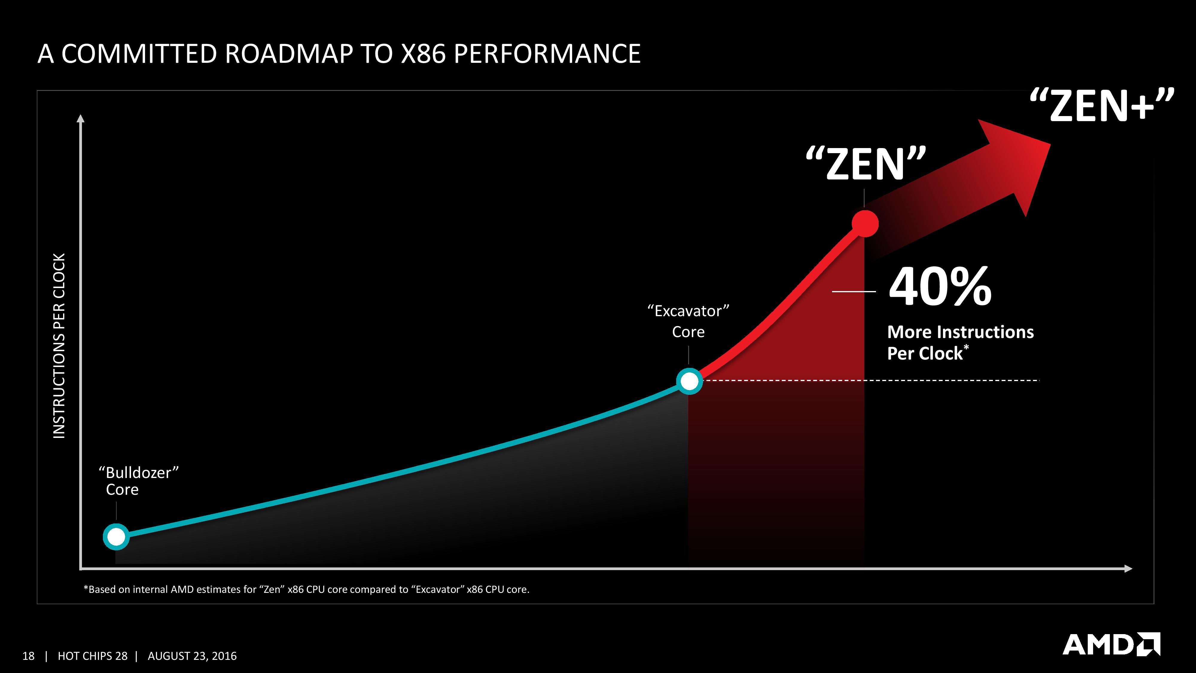
We are told that AMD has a clear internal roadmap for CPU microarchitecture design over the next few generations. As long as we don’t stay for so long on 14nm similar to what we did at 28/32nm, with IO updates over the coming years, a competitive clock-for-clock product (even to Broadwell) with good efficiency will be a welcome return.


106 Comments
View All Comments
Xajel - Wednesday, August 24, 2016 - link
I have a feeling that the Socket has more potential, there's a huge jump in pin counts that might hides something, I suspect AMD have specific HEDT version with higher TDP ( like 130-140 ) that might ship later in 2017 after the first wave. or maybe even triple channel that works only on higher-end HEDT motherboard while it will be still backward compatible with regular dual channels motherboards...none12345 - Wednesday, August 24, 2016 - link
Nice article, thanks, and timely too.Cant wait for real zen benchmarks.
I so badly want this to be another athlon64 x2 moment. But i dont think we will get that, and we don't need that. Consider the athlon 64 gave us multicore, and it stomped the pentium4 as well.
Ill be completey happy with a phenom II moment. Which was note quite as fast as intel, but gave you more almost as fast cores for your money. As well as unlocking cores at a much lower price point, which gave you superior overclocking for your money.
I will not at this point consider buying another quad core. Quad core is insufficient for my typical work load. I do not use 1 heavily multithreaded piece of software, i constantly use multiple pieces of moderately threaded software that currently mostly maxes out my processor.
In my opinion the industry should have stopped selling dual cores a year ago. It should be quad core at the low end and 6 or 8 core should be the mainstream. For desktop that is, i can still see some moble things being dual core.
Because i will NOT consider another quad core at this point. My only option today is the intel's enthusiast platform, which is far too expensive relative to the performance increase. So they are out.
And this is why im hoping that zen does not disappoint. If they can give me 6 or 8 cores that are within 10% per core, for similar costs to the i5 or i7 line, then im a definite buy. If they give me 6 or 8 cores that are priced like intel's enthusiast platform, well then i guess im not upgrading, untill someone can offer me more cores for a reasonable price.
If intel would offer more cores mainstream, then id absolutely consider a new chip from them. IE if i3 was 4 core, i5 was 6 core, and i7 was 8 core.
Vlad_Da_Great - Wednesday, August 24, 2016 - link
i7-4790K will wipe the floor with the ZEN mop. Roy Jones Jr(Intel) vs Montell Griffin(AMD) part II. https://www.youtube.com/watch?v=VZ_4FrhHHJE That is it! I cant believe AnandTech is biting on their marketing fluff.H2323 - Wednesday, August 24, 2016 - link
"Nevertheless, power was the main concern rather than pure performance or function, which have been typical AMD targets in the past."This is contradictory to what AMD has had to say. Power was not a greater focus than performance, just not true.
takeshi7 - Wednesday, August 24, 2016 - link
Wow, I haven't seen victim caches being used in a CPU since the old VIA C3. I hope the advantage of not having to duplicate data between the L2 and L3 caches pays off for AMD.H2323 - Wednesday, August 24, 2016 - link
and bulldozer in 2011Oxford Guy - Saturday, August 27, 2016 - link
The EDRAM L4 in Broadwell C is supposed to be a victim cache.intangir - Wednesday, August 24, 2016 - link
Great article. By the way, Ian, you're missing a syllable from "Microarchitecture" in the title.name99 - Wednesday, August 24, 2016 - link
"The first, CLZERO, is aimed to clear a cache line and is more aimed at the data center and HPC crowds"Not exactly. The point of an instruction like CLZERO is that the usual way cache lines are filled uses twice as much bandwidth as necessary.
When I write the first datum to a cacheline, the first thing that needs to be done is to load the cacheline and then overwrite the datum I wanted to write. This is obvious. BUT suppose I'm writing enough data that I write over the entire cache line? Then pulling it in was a waste of bandwidth.
THAT is the point of an instruction like CLZERO, to "ready the cache line for being overwritten" without wasting time loading it. Of course for many purposes filling with zeros is what one wants, but there are other times when one is simply engaged in bulk writing and it again makes sense.
PPC for example had a similar instruction, DCBZ, as does ARM, DC ZVA.
I'd expect this instruction to be used, at the absolute minimum, by the OS wherever it needs to zero and copy pages, by standard libraries data copy routines, and by the compiler whenever it writes "large" (ie cache line or larger) data structures.
"PTE (Page Table Entry) Coalescing is the ability to combine small 4K page tables into 32K page tables, and is a software transparent implementation. This is useful for reducing the number of entries in the TLBs and the queues, but requires certain criteria of the data to be used within the branch predictor to be met."
I think you are misunderstanding what this is about. My GUESS (only a guess) is that it refers to the following.
Academic work was done a few years ago that showed that the way Linux (and probably most other OSs) allocated and deallocated pages meant that, for the most part, contiguous virtual pages remain as contiguous physical pages over reasonably long stretches (say 8 to 16 pages). A consequence of this is that a TLB entry could contain not just the single physical address it refers to but also a length field or something equivalent, say that this TLB holds for this page and, say, the next 5 pages. This would work IF
- the pages all have the same settings and permissions (usually the case)
- the pages are contiguous in physical memory (as I said, usually the case)
The consequence of this is that for fairly minor modifications to the TLB, one manages to double or more the coverage of one's TLB, and that's certainly nothing to be sneered at.
It's possible that an OS that tries to maintain page contiguity could do even better --- the papers I read referred to unmodified Linux.
I've no idea what that branch predictor info refers to; but perhaps this is more of the usual x86 BS where you have to deal with some insane corner condition involving self-modifying code. The basic point, however, is obvious --- you get a nice increase in TLB coverage without having to change software, and without the pain of jumping to a larger page size.
I'm really glad to see AMD implement this because I thought it was a nice idea when I read it, and it's basically useful for everyone ---also IBM, also Intel, also ARM --- as long as the OS you're running is not insane. For someone like Apple, where they can fully control the OS, it's especially appealing. (And hell, for all we know they're actually first before AMD, they just never told anyone?)
name99 - Wednesday, August 24, 2016 - link
here we are, this is the paper I was referring to:http://www.cs.rutgers.edu/~abhib/binhpham-micro12....