AMD Zen Microarchiture Part 2: Extracting Instruction-Level Parallelism
by Ian Cutress on August 23, 2016 8:45 PM EST- Posted in
- CPUs
- AMD
- x86
- Zen
- Microarchitecture
Execution, Load/Store, INT and FP Scheduling
The execution of micro-ops get filters into the Integer (INT) and Floating Point (FP) parts of the core, which each have different pipes and execution ports. First up is the Integer pipe which affords a 168-entry register file which forwards into four arithmetic logic units and two address generation units. This allows the core to schedule six micro-ops/cycle, and each execution port has its own 14-entry schedule queue.
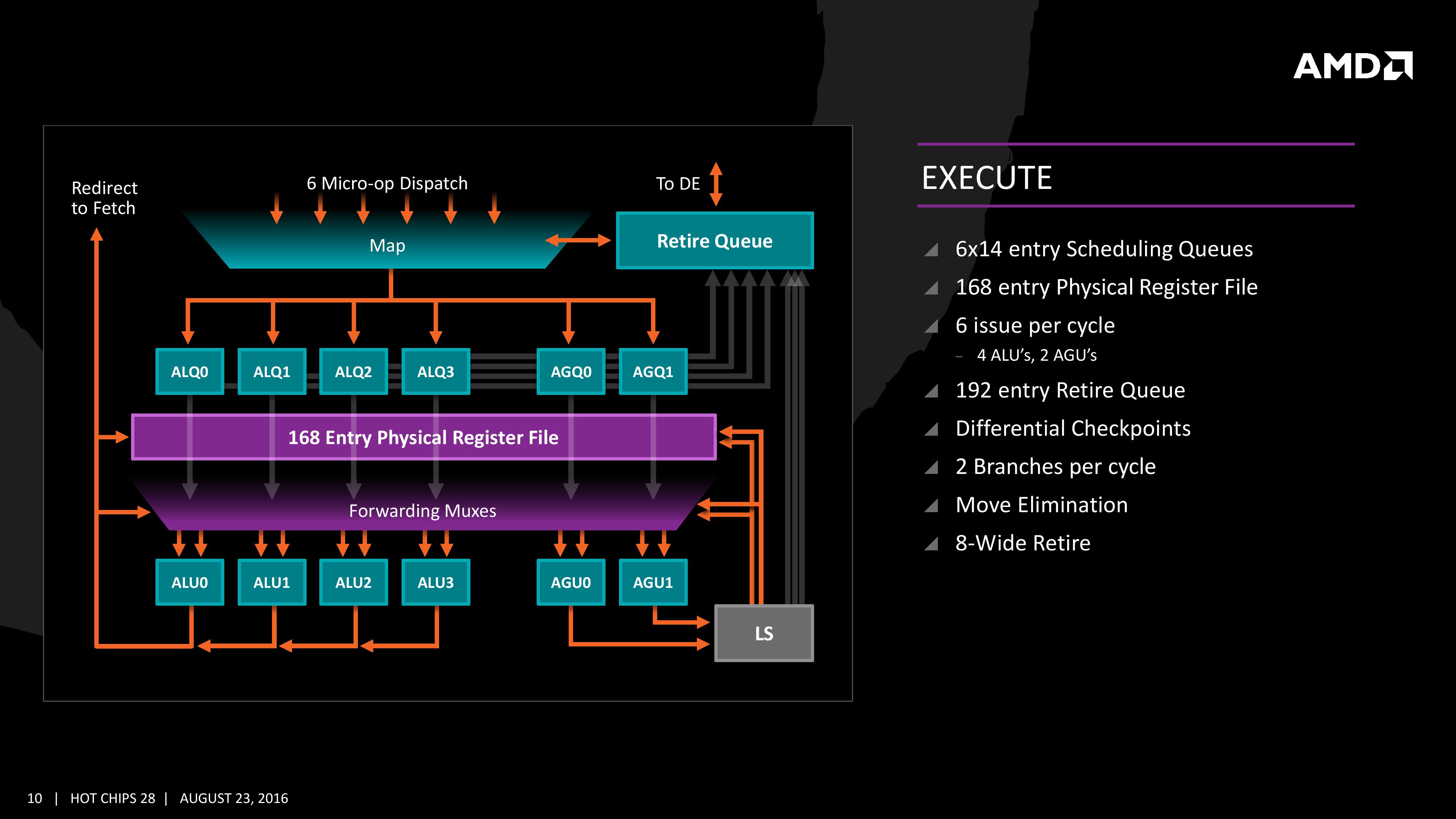
The INT unit can work on two branches per cycle, but it should be noted that not all the ALUs are equal. Only two ALUs are capable of branches, one of the ALUs can perform IMUL operations (signed multiply), and only one can do CRC operations. There are other limitations as well, but broadly we are told that the ALUs are symmetric except for a few focused operations. Exactly what operations will be disclosed closer to the launch date.
The INT pipe will keep track of branching instructions with differential checkpoints, to cut down on storing redundant data between branches (saves queue entries and power), but can also perform Move Elimination. This is where a simple mov command between two registers occurs – instead of inflicting a high energy loop around the core to physically move the single instruction, the core adjusts the pointers to the registers instead and essentially applies a new mapping table, which is a lower power operation.
Both INT and FP units have direct access to the retire queue, which is 192-entry and can retire 8 instructions per cycle. In some previous x86 CPU designs, the retire unit was a limiting factor for extracting peak performance, and so having it retire quicker than dispatch should keep the queue relatively empty and not near the limit.
The Load/Store Units are accessible from both AGUs simultaneously, and will support 72 out-of-order loads. Overall, as mentioned before, the core can perform two 16B loads (2x128-bit) and one 16B store per cycle, with the latter relying on a 44-entry Store queue. The TLB buffer for the L2 cache for already decoded addresses is two level here, with the L1 TLB supporting 64-entry at all page sizes and the L2 TLB going for 1.5K-entry with no 1G pages. The TLB and data pipes are split in this design, which relies on tags to determine if the data is in the cache or to start the data prefetch earlier in the pipeline.
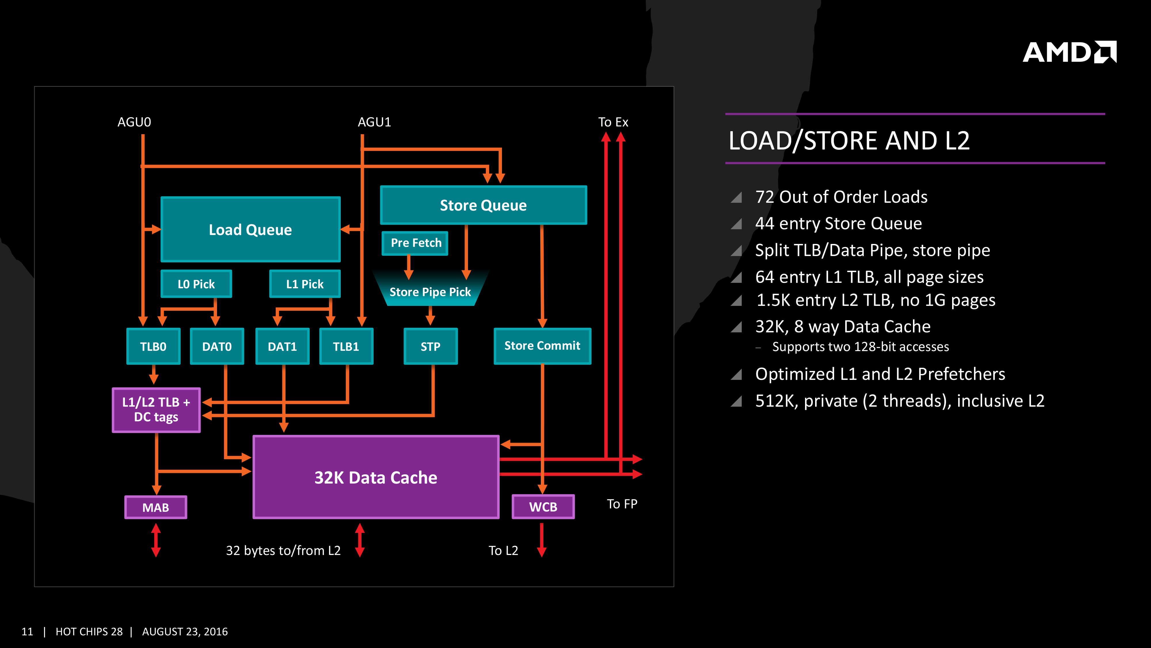
The data cache here also has direct access to the main L2 cache at 32 Bytes/cycle, with the 512 KB 8-way L2 cache being private to the core and inclusive. When data resides back in L1 it can be processed back to either the INT or the FP pipes as required.
Moving onto the floating point part of the core, and the first thing to notice is that there are two scheduling queues here. These are listed as ‘schedulable’ and ‘non-schedulable’ queues with lower power operation when certain micro-ops are in play, but also allows the backup queue to sort out parts of the dispatch in advance via the LDCVT. The register file is 160 entry, with direct FP to INT transfers as required, as well as supporting accelerated recovery on flushes (when data is written to a cache further back in the hierarchy to make room).
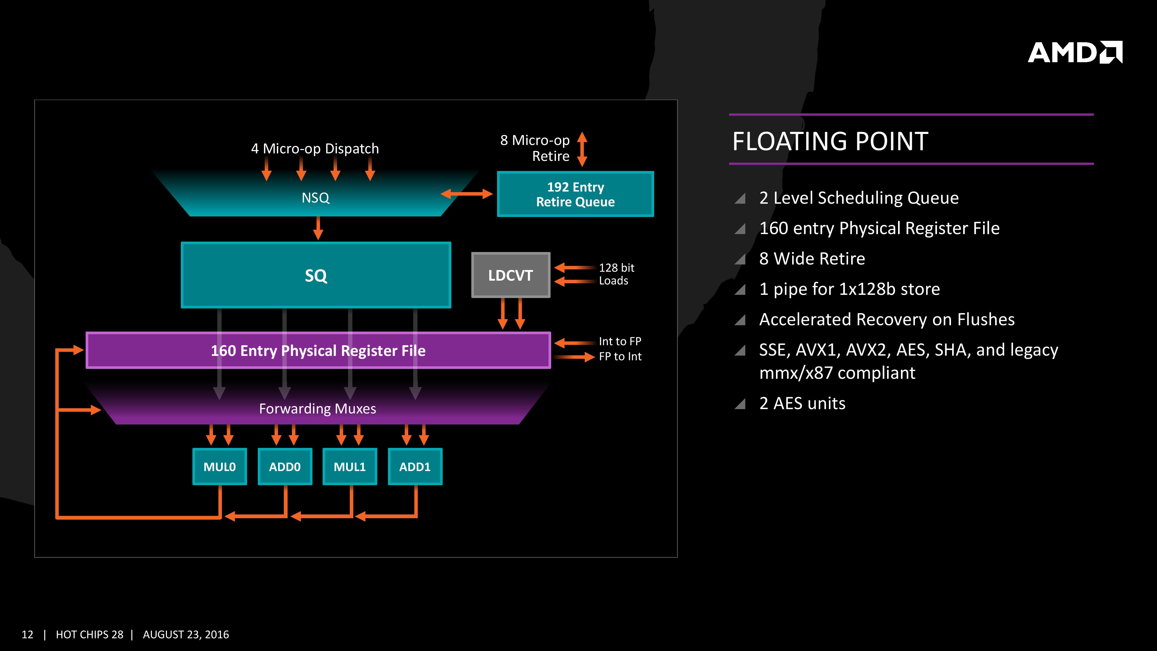
The FP Unit uses four pipes rather than three on Excavator, and we are told that the latency in Zen is reduced as well for operations (though more information on this will come at a later date). We have two MUL and two ADD in the FP unit, capable of joining to form two 128-bit FMACs, but not one 256-bit AVX. In order to do AVX, the unit will split the operations accordingly. On the counter side each core will have 2 AES units for cryptography as well as decode support for SSE, AVX1/2, SHA and legacy mmx/x87 compliant code.


106 Comments
View All Comments
Xajel - Wednesday, August 24, 2016 - link
I have a feeling that the Socket has more potential, there's a huge jump in pin counts that might hides something, I suspect AMD have specific HEDT version with higher TDP ( like 130-140 ) that might ship later in 2017 after the first wave. or maybe even triple channel that works only on higher-end HEDT motherboard while it will be still backward compatible with regular dual channels motherboards...none12345 - Wednesday, August 24, 2016 - link
Nice article, thanks, and timely too.Cant wait for real zen benchmarks.
I so badly want this to be another athlon64 x2 moment. But i dont think we will get that, and we don't need that. Consider the athlon 64 gave us multicore, and it stomped the pentium4 as well.
Ill be completey happy with a phenom II moment. Which was note quite as fast as intel, but gave you more almost as fast cores for your money. As well as unlocking cores at a much lower price point, which gave you superior overclocking for your money.
I will not at this point consider buying another quad core. Quad core is insufficient for my typical work load. I do not use 1 heavily multithreaded piece of software, i constantly use multiple pieces of moderately threaded software that currently mostly maxes out my processor.
In my opinion the industry should have stopped selling dual cores a year ago. It should be quad core at the low end and 6 or 8 core should be the mainstream. For desktop that is, i can still see some moble things being dual core.
Because i will NOT consider another quad core at this point. My only option today is the intel's enthusiast platform, which is far too expensive relative to the performance increase. So they are out.
And this is why im hoping that zen does not disappoint. If they can give me 6 or 8 cores that are within 10% per core, for similar costs to the i5 or i7 line, then im a definite buy. If they give me 6 or 8 cores that are priced like intel's enthusiast platform, well then i guess im not upgrading, untill someone can offer me more cores for a reasonable price.
If intel would offer more cores mainstream, then id absolutely consider a new chip from them. IE if i3 was 4 core, i5 was 6 core, and i7 was 8 core.
Vlad_Da_Great - Wednesday, August 24, 2016 - link
i7-4790K will wipe the floor with the ZEN mop. Roy Jones Jr(Intel) vs Montell Griffin(AMD) part II. https://www.youtube.com/watch?v=VZ_4FrhHHJE That is it! I cant believe AnandTech is biting on their marketing fluff.H2323 - Wednesday, August 24, 2016 - link
"Nevertheless, power was the main concern rather than pure performance or function, which have been typical AMD targets in the past."This is contradictory to what AMD has had to say. Power was not a greater focus than performance, just not true.
takeshi7 - Wednesday, August 24, 2016 - link
Wow, I haven't seen victim caches being used in a CPU since the old VIA C3. I hope the advantage of not having to duplicate data between the L2 and L3 caches pays off for AMD.H2323 - Wednesday, August 24, 2016 - link
and bulldozer in 2011Oxford Guy - Saturday, August 27, 2016 - link
The EDRAM L4 in Broadwell C is supposed to be a victim cache.intangir - Wednesday, August 24, 2016 - link
Great article. By the way, Ian, you're missing a syllable from "Microarchitecture" in the title.name99 - Wednesday, August 24, 2016 - link
"The first, CLZERO, is aimed to clear a cache line and is more aimed at the data center and HPC crowds"Not exactly. The point of an instruction like CLZERO is that the usual way cache lines are filled uses twice as much bandwidth as necessary.
When I write the first datum to a cacheline, the first thing that needs to be done is to load the cacheline and then overwrite the datum I wanted to write. This is obvious. BUT suppose I'm writing enough data that I write over the entire cache line? Then pulling it in was a waste of bandwidth.
THAT is the point of an instruction like CLZERO, to "ready the cache line for being overwritten" without wasting time loading it. Of course for many purposes filling with zeros is what one wants, but there are other times when one is simply engaged in bulk writing and it again makes sense.
PPC for example had a similar instruction, DCBZ, as does ARM, DC ZVA.
I'd expect this instruction to be used, at the absolute minimum, by the OS wherever it needs to zero and copy pages, by standard libraries data copy routines, and by the compiler whenever it writes "large" (ie cache line or larger) data structures.
"PTE (Page Table Entry) Coalescing is the ability to combine small 4K page tables into 32K page tables, and is a software transparent implementation. This is useful for reducing the number of entries in the TLBs and the queues, but requires certain criteria of the data to be used within the branch predictor to be met."
I think you are misunderstanding what this is about. My GUESS (only a guess) is that it refers to the following.
Academic work was done a few years ago that showed that the way Linux (and probably most other OSs) allocated and deallocated pages meant that, for the most part, contiguous virtual pages remain as contiguous physical pages over reasonably long stretches (say 8 to 16 pages). A consequence of this is that a TLB entry could contain not just the single physical address it refers to but also a length field or something equivalent, say that this TLB holds for this page and, say, the next 5 pages. This would work IF
- the pages all have the same settings and permissions (usually the case)
- the pages are contiguous in physical memory (as I said, usually the case)
The consequence of this is that for fairly minor modifications to the TLB, one manages to double or more the coverage of one's TLB, and that's certainly nothing to be sneered at.
It's possible that an OS that tries to maintain page contiguity could do even better --- the papers I read referred to unmodified Linux.
I've no idea what that branch predictor info refers to; but perhaps this is more of the usual x86 BS where you have to deal with some insane corner condition involving self-modifying code. The basic point, however, is obvious --- you get a nice increase in TLB coverage without having to change software, and without the pain of jumping to a larger page size.
I'm really glad to see AMD implement this because I thought it was a nice idea when I read it, and it's basically useful for everyone ---also IBM, also Intel, also ARM --- as long as the OS you're running is not insane. For someone like Apple, where they can fully control the OS, it's especially appealing. (And hell, for all we know they're actually first before AMD, they just never told anyone?)
name99 - Wednesday, August 24, 2016 - link
here we are, this is the paper I was referring to:http://www.cs.rutgers.edu/~abhib/binhpham-micro12....