The Intel Xeon E5 v4 Review: Testing Broadwell-EP With Demanding Server Workloads
by Johan De Gelas on March 31, 2016 12:30 PM EST- Posted in
- CPUs
- Intel
- Xeon
- Enterprise
- Enterprise CPUs
- Broadwell
A Modest Tick
As Broadwell is a tick - a die shrink of an existing architecture, rather than a new architecture - so you should expect modest IPC improvements. Most Xeon E5 v4 SKUs have slightly lower clockspeeds compared to their Haswell v3 brethren, so overall the single threaded performance has hardly improved. Clock for clock, Intel tells us that their simulation tools show that Broadwell delivers about 5% better performance per clock in non-AVX2 traces.
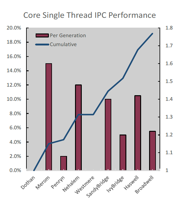
First Y-axis + bars: simulated single threaded performance improvement. Blue line + second Y-axis is the cumulative improvement.
In that sense, Broadwell is basically a Haswell made on Intel's 14nm second generation tri-gate transistor process. Intel did make a few subtle improvements to the micro-architecture:
- Faster divider: lower latency & higher throughput
- AVX multiply latency has decreased from 5 to 3
- Bigger TLB (1.5k vs 1k entries)
- Slightly improved branch prediction (as always)
- Larger scheduler (64 vs 60)
None of these improvements will yield large performance improvements. The larger improvements must come from other features.
New Features
Compared to Haswell-EP, Broadwell-EP also includes some new features. The first one is the improved power control unit.
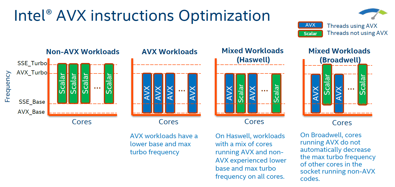
On Haswell, one AVX instruction on one core forced all cores on the same socket to slow down their clockspeed by around 2 to 4 speed bins (-200,-400 MHz) for at least 1 ms, as AVX has a higher power requirement that reduces how much a CPU can turbo. On Broadwell, only the cores that run AVX code will be reducing their clockspeed, allowing the other cores to run at higher speeds.
The other performance feature is the vastly improved PCLMULQDQ (carry-less multiplication) instruction: throughput has been doubled, and latency reduced from 7 cycles to 5.
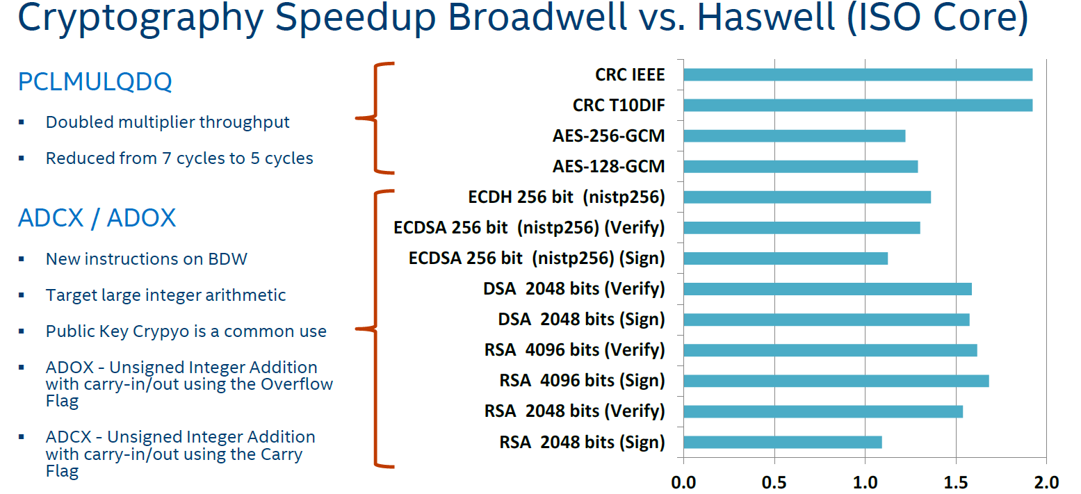
This increases AES (symmetric) encryption performance by 20-25%, and CRCs (Cyclic Redundancy check) are up to 90% faster. Broadwell also has some new ADCX/ADOX instructions to speed up asymmetric encryption algorithms such as the popular RSA. These improvements are implemented in OpenSSL 1.0.2-beta3. But don't expect too much from it.. The compute intensive asymetric encryption is mostly used to initiate a secure connection. Most modern web applications keep their sessions "alive", and as a result, events that require asymmetric encryption happen a lot less frequentely . Symmetric encryption (like AES) which is used to send encrypted data is a lot lighter, so even on a fully encrypted website with long encrypted data streams, encryption is only a small percentage (<5%) of the total computing load.


112 Comments
View All Comments
Kevin G - Thursday, March 31, 2016 - link
Much like how Apple skipped Haswell-EP, they also skipped a generation of cards from AMD and nVidia. So even if Apple doesn't wait for new GPUs, their is certainly an update on the GPU side.The more interesting possibility would be if Apple were to go with Xeon D in the Mac Pro instead of Broadwell-EP. Apple would need a big PLX chip considering the number of lanes they's want to use but it is possible.
bill.rookard - Thursday, March 31, 2016 - link
Another issue is that they're not under any pressure from any competition to really innovate. I don't even remember the last time I read anything about Opteron servers... let alone something about any NEW Opterons.ComputerGuy2006 - Thursday, March 31, 2016 - link
A sign of things to come for Broadwell-e?Seems like a tricky situation. Because skylake-e will come with a new platform in 2017, while broadwell-e isn't the fastest IPC and there are crazy rumors it will might cost $1500 (lol Intel). We also have Zen later this year that might give good performance with good cost/perf ratio.
extide - Thursday, March 31, 2016 - link
Yeah so Intel only gives us the LCC part for the -E platform, so we will see the 10-core SKU as the top, It will either be $1000, or $1500 ... so yeah not sure how that will end up. Although there will be 8 and 6 core options that should be pretty affordable.Hopefully they do an 8 core part with 28 lanes for under $500, as THAT would be a great deal!
dragonsqrrl - Sunday, April 3, 2016 - link
I'm hoping the 8 core SKU is around $600, the position the x930K traditionally occupies. What makes me a little worried is that there will be 4 SKUs instead of 3 this time (one 10 core, one 8 core, and two 6 core), and I'm not sure there's enough room under the $600 price point for two 6 core processors.jasonelmore - Thursday, March 31, 2016 - link
Can it run Star Citizen?theduckofdeath - Thursday, March 31, 2016 - link
A question we'll never get an answer to? :DJohanAnandtech - Friday, April 1, 2016 - link
It probably runs mostly on Xeons. Well, the back end that is :-)extide - Thursday, March 31, 2016 - link
BOOM, 454mm^2 on the worlds best process. The "other" 14/16nm processes use bigger geometry than Intel's 14nm process.Now we just need those other guys to catch up so we can see 450+mm GPU's!
Kevin G - Thursday, March 31, 2016 - link
Intel still has plenty of room to increase die size. The largest chip they've produced was the Tukwila Itanium 2 at 699 mm^2. Granted that was a 65 nm design but Haswell-EX is a juggarnaught at 662 mm^2 on Intel's more recent 22 nm process. Seems reasonable that SkyLake-EX could go to 32 cores as Intel has >200 mm^2 of rectal limit left.As for GPU's, they're also huge. nVidia's GM200 is 601 mm^2 and AMD's Fiji is 'only' 596 mm^2 both on 28 nm process. TSMC's 20 nm process was skipped so even using the looser 16 nm FinFET, GPU's will see a significant shrink compared to the those high end chips.