We were initially concerned with how the flip-chip MAP GeForce4 440 Go 64MB would be cooled, but NVIDIA ensured us that cooling on the bottom of the chip is not necessary. The entire GeForce4 Go line includes no connect balls on the bottom that help transfer heat from the core to the surrounding area. What's more, the 31x31 package that NVIDIA began to use in the GeForce4 Go line is going to be a standard adopted by NVIDIA, meaning that the next generation mobile chip will be the same size and have the same pin-outs as the current GeForce4 Go chips. This should make upgrades for OEMs easy, allowing them to upgrade older models to newer video technology without completely reworking the system. Looking for proof that NVIDIA is sticking to this configuration for a while? The current GeForce4 Go package includes pins for AGP 8X, meaning that as soon as the hardware can handle the new spec, so can the package.
The following table should prove to be useful in distinguishing the various breeds of GeForce4 Go chips, as each runs at a different clock speed and uses a different memory bus.
|
GeForce4
Go Chips
|
||||||||
|
GeForce4
440 Go
|
GeForce4
440 Go 64MB
|
GeForce4
420 Go
|
GeForce4
420 Go 32MB
|
GeForce4
410 Go 16MB
|
||||
| Package Size | 31mm x 31mm | 31mm x 31mm | 23mm x 23mm | 31mm x 31mm | 31mm x 31mm | |||
|
Package Type |
Discrete | MAP | Discrete | MAP | MAP | |||
| On Chip Memory | N/A | 64MB | N/A | 32MB | 16MB | |||
| Core Clock | 220MHz | 190MHz | 200MHz | 190MHz | 190MHz | |||
| Fill Rate | 880M texels/sec | 760M texels/sec | 800M texels/sec | 760M texels/sec | 760M texels/sec | |||
| Memory Bus | 128-bit DDR | 128-bit DDR | 64-bit DDR | 64-bit DDR | 64-bit SDR | |||
| Memory Clock | 220MHz DDR (440MHz) | 200MHz DDR (400MHz) | 200MHz DDR (400MHz) | 200MHz DDR (400MHz) | 200MHz SDR (400MHz) | |||
| Memory Bandwidth | 7.0GB/s | 6.4GB/s | 3.2GB/s | 3.2GB/s |
1.6GB/s |
|||
As you can see, the GeForce4 Go chips run at different speeds depending on their package type. All the MAP solutions run at 190MHz/200MHz and are only differentiated by the amount of memory they incorporate and the memory bus width used. The discrete GeForce4 Go chips are clocked slightly differently: 220MHz/220MHz on the discreet GeForce4 440 Go and 200MHz/200MHz on the discrete GeForce4 420 Go. Since both discrete GeForce4 Go chips are clocked differently than their MAP counterpart, performance of the chip will differ depending on the chip package an OEM chooses to use. Not all GeForce4 440 Go and GeForce4 420 Go chips will perform the same: the discrete solutions should perform slightly faster than the MAP ones.
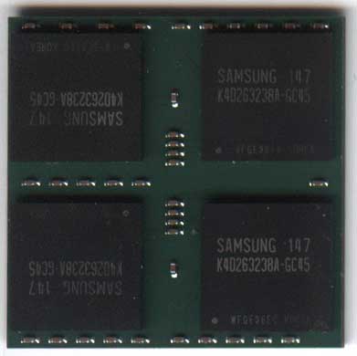
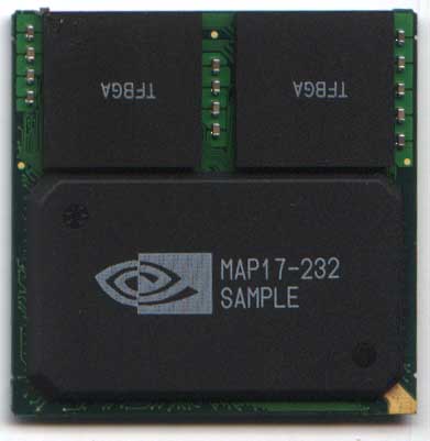
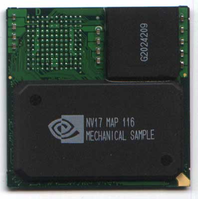
Below you can see pictures of the NVIDIA GeForce4 Go chip line, with the exception of the discrete GeForce4 420 Go. Keep in mind that this chip with its 23mm x 23mm package is smaller than the remainder of the line.
|
MAP
GeForce4 440 Go 64MB
|
|
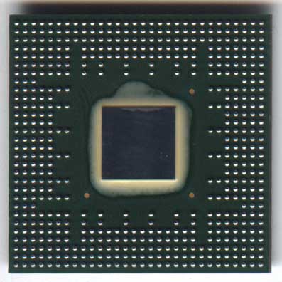
Discrete GeForce4 440
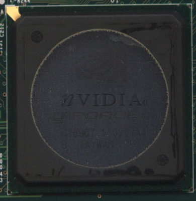
Click here to enlarge.
|
MAP
GeForce4 420 Go 32MB
|
|

|
MAP
GeForce4 410 Go 16MB
|
|


0 Comments
View All Comments