The ARM vs x86 Wars Have Begun: In-Depth Power Analysis of Atom, Krait & Cortex A15
by Anand Lal Shimpi on January 4, 2013 7:32 AM EST- Posted in
- Tablets
- Intel
- Samsung
- Arm
- Cortex A15
- Smartphones
- Mobile
- SoCs
Determining the TDP of Exynos 5 Dual
Throughout all of our Cortex A15 testing we kept bumping into that 4W ceiling with both the CPU and GPU - but we rarely saw both blocks use that much power at the same time. Intel actually tipped me off to this test to find out what happens if we try and force both the CPU and GPU to run at max performance at the same time. The graph below is divided into five distinct sections, denoted by colored bars above the sections. On this chart I have individual lines for GPU power consumption (green), CPU power consumption (blue) and total platform power consumption, including display, measured at the battery (red).
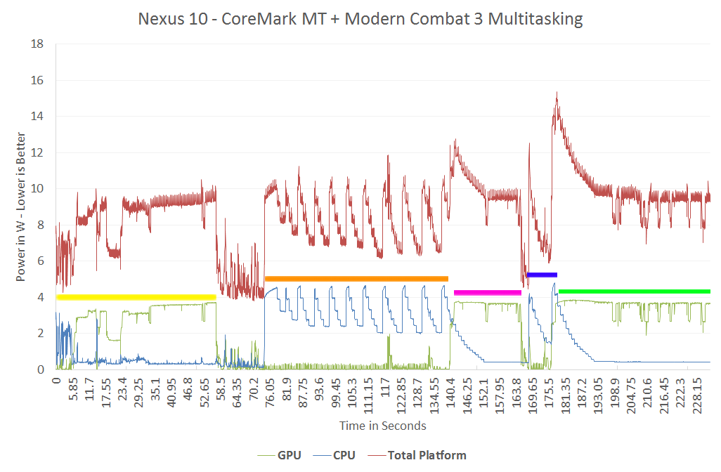
In the first section (yellow), we begin playing Modern Combat 3 - a GPU intensive first person shooter. GPU power consumption is just shy of 4W, while CPU power consumption remains below 1W. After about a minute of play we switch away from MC3 and you can see both CPU and GPU power consumption drop considerably. In the next section (orange), we fire up a multithreaded instance of CoreMark - a small CPU benchmark - and allow it to loop indefinitely. CPU power draw peaks at just over 4W, while GPU power consumption is understandably very low.
Next, while CoreMark is still running on both cores, we switch back to Modern Combat 3 (pink section of the graph). GPU voltage ramps way up, power consumption is around 4W, but note what happens to CPU power consumption. The CPU cores step down to a much lower voltage/frequency for the background task (~800MHz from 1.7GHz). Total SoC TDP jumps above 4W but the power controller quickly responds by reducing CPU voltage/frequency in order to keep things under control at ~4W. To confirm that CoreMark is still running, we then switch back to the benchmark (blue segment) and you see CPU performance ramps up as GPU performance winds down. Finally we switch back to MC3, combined CPU + GPU power is around 8W for a short period of time before the CPU is throttled.
Now this is a fairy contrived scenario, but it's necessary to understand the behavior of the Exynos 5250. The SoC is allowed to reach 8W, making that its max TDP by conventional definitions, but seems to strive for around 4W as its typical power under load. Why are these two numbers important? With Haswell, Intel has demonstrated interest (and ability) to deliver a part with an 8W TDP. In practice, Intel would need to deliver about half that to really fit into a device like the Nexus 10 but all of the sudden it seems a lot more feasible. Samsung hits 4W by throttling its CPU cores when both the CPU and GPU subsystems are being taxed, I wonder what an 8W Haswell would look like in a similar situation...


140 Comments
View All Comments
powerarmour - Friday, January 4, 2013 - link
So yes, finally confirming what anyone with half a brain knows, competitive ARM SoC's use less power.apinkel - Friday, January 4, 2013 - link
I'm assuming you are kidding.Atom is roughly equivalent to (dual core) Krait in power draw but has better performance.
The A15 is faster than either krait or the atom but it's power draw is too much to make it usable in a smartphone (which is I'm assuming why qualcomm had to redesign the A15 architecture for krait to make it fit into the smartphone power envelope).
The battle I still want to see is quad core krait and atom.
ImSpartacus - Friday, January 4, 2013 - link
Let me make sure I have this straight. Did Qualcomm redesign A15 to create Krait?djgandy - Friday, January 4, 2013 - link
No. Qualcomm create their own designs from scratch. They have an Instruction Set licence for ARM but they are arm "clones"apinkel - Friday, January 4, 2013 - link
Sorry, yeah, I could have worded that better.But in any case the comment now has me wondering if I'm off base in my understanding of how Qualcomm does what it does...
I've been under the impression that Qualcomm took the ARM design and tweaked it for their needs (instead of just licensing the instruction set and the full chip design top to bottom). Yeah/Nay?
fabarati - Friday, January 4, 2013 - link
Nay.They do what AMD does, they license the instruction set and create their own cpus that are compatible with the ARM ISA's (in Krait's case, the ARMv7). That's also what Apple did with their Swift cores.
Nvidia tweaked the Cortex A9 in the Tegra 2, but it was still a Cortex A9. Ditto for Samsung, Hummingbird and the Cortex A8.
designerfx - Friday, January 4, 2013 - link
do I need to remind you that the Tegra 3 has disabled cores on the RT? Using an actual android device with Tegra 3 would show better results.madmilk - Friday, January 4, 2013 - link
The disabled 5th core doesn't matter in loaded situations. During idle, screen power dominates, so it still doesn't really matter. About all you'll get is more standby time, and Atom seems to be doing fine there.designerfx - Friday, January 4, 2013 - link
The core allows a lot of different significant things - so in other words, it's extremely significant, including in high load situations as well.That has nothing to do with the Atom. You get more than standby time.
designerfx - Friday, January 4, 2013 - link
also, during idle the screen is off, usually after whatever amount of time the settings are set for. Which is easily indicated in the idle measurements. What the heck are you even talking about?