ASUS V7700 Deluxe 32MB GeForce2 GTS
by Vlad Trishkin on November 3, 2000 12:55 AM EST- Posted in
- GPUs
The Card
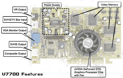
The layout of the board is similar to that of the V6800, and the one of the most noticeable changes is the shape of the current heatsink/fan. Both boards actually use similar reference designs, and each card occupies about 27 square inches of silicon. If you take the V7700 and the V6800 side by side you will not notice any major changes, except for a few capacitators, and connector locations. ASUS has managed to fit a lot on this PCB, without any wasted space. The board is actually quite "busy" in terms of "Parts per square inch". ASUS has not followed NVIDIA's suggested PCB reference design, and has created their own, largely due to the added video components. Hardware monitoring is regulated via the Winbond W837D chip, which reports the overall condition of the card, and can be monitored with the help of ASUS software.
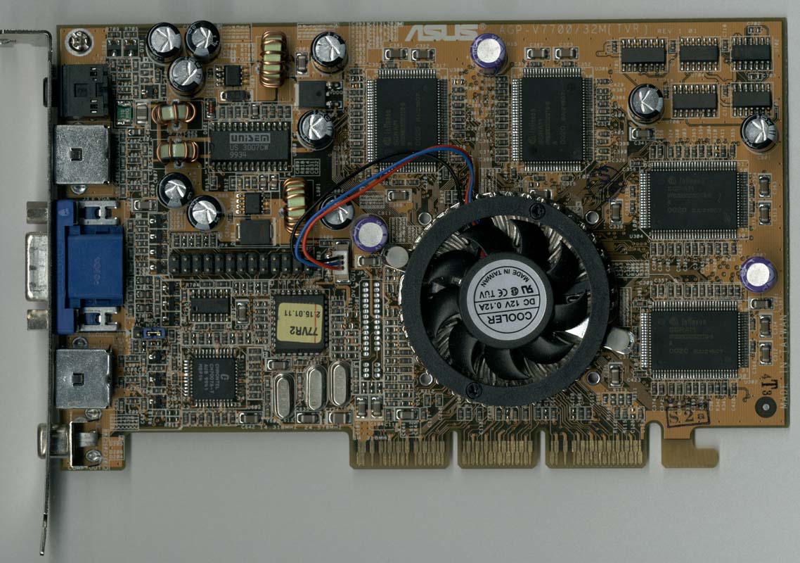
The latest NVIDIA 0.18-micron GeForce2 GTS core powers the V7700, apposed to the original GeForce 256 core found on the V6800. Our test card came with a very nice heatsink and a fan, which handles the job of dissipating heat. The heatsink is stiffly seated on top of the chip, and is attached with a simple metal clip mechanism. ASUS didn't overlook any details, and has applied a respectable amount of thermal heat-transfer grease for better heat conductivity between the core-plate and the heatsink, which will ultimately result in better heat dissipation. The core is clocked at a standard speed of 200MHz, but by the looks of it can do a lot better.
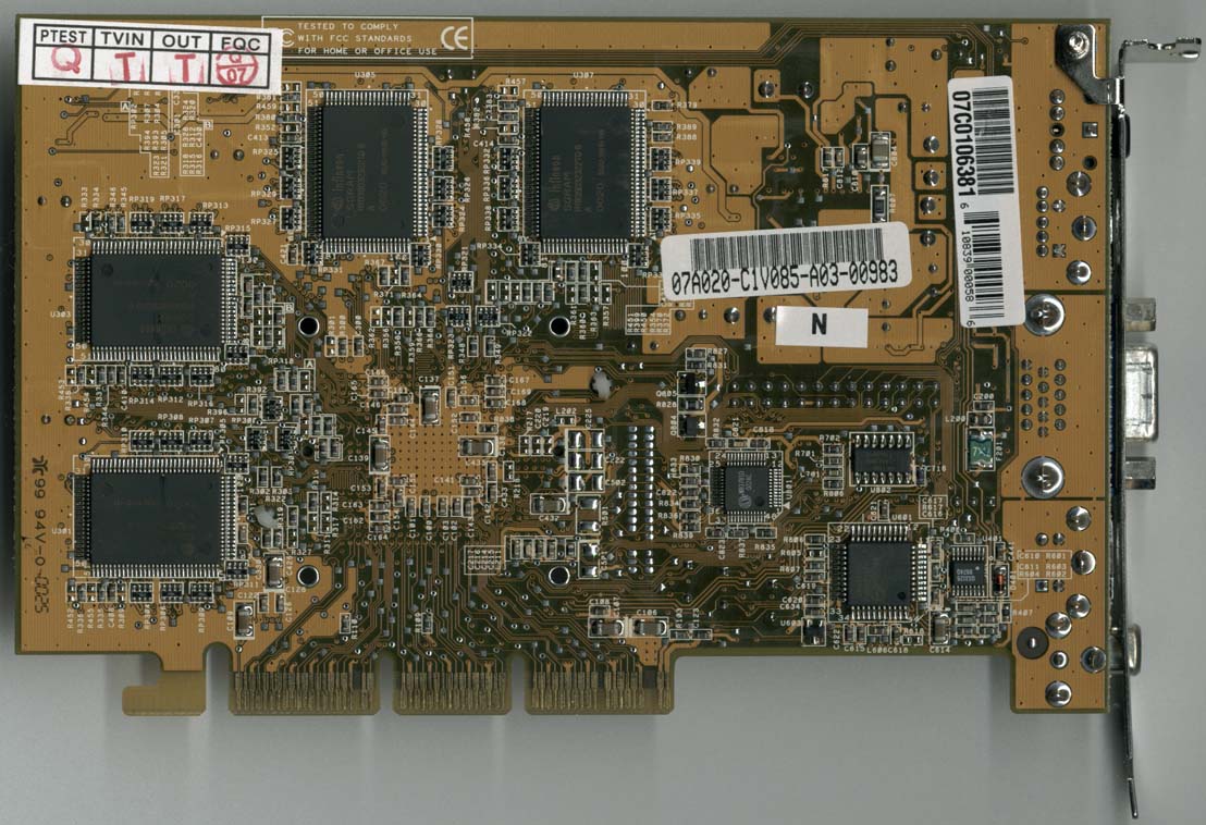
The memory has not changed much, The V7700 and the V6800 use similar SGRAM,
the only difference is that the new memory is clocked 16 more MHz DDR. The memory
is divided between (8) 4MB chips on front and back of the card. Our card came
with Infineon 6'ns SGRAM, which is standard for most GeForce 2 cards out there.


0 Comments
View All Comments