Sandy Bridge-E and X79 – The ASUS P9X79 PRO Review
by Ian Cutress on November 14, 2011 3:01 AM EST- Posted in
- Motherboards
- Asus
- X79
It seems that every few months or so, we get a new socket and a slew of new chipsets from Intel. If we go back as far as 775 (mainstream), in consumer land, we have covered 1366 (enthusiast), 1156 (mainstream) and 1155 (mainstream). This is in contrast to AMD’s backwards compatibility progression of AM2/AM2+ to AM3/AM3+ (if you ignore Llano and Fusion).
Information has been flying around about the new X79 enthusiast platform for some months now, especially when looking for a replacement for X58. Needless to say, X79 aims at high end and high price. There are the main changes that everyone knows and cares about – quad channel memory and 40 PCIe lanes strike high on anyone’s list about X79. Does that mean the chipset is really for those who want >16 GB of memory, or 2/3 way GPU action?
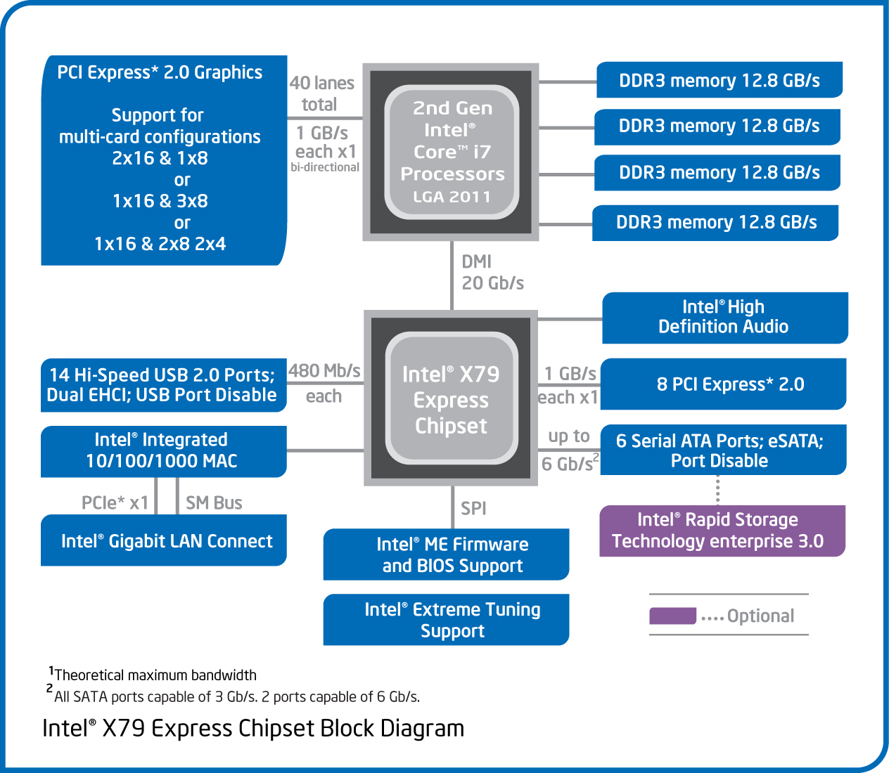
 Block Diagram.png)
Above is a block diagram of the routing of the LGA 2011 socket and the X79 Platform Controller Hub (PCH), taken from Intel’s DX79SI motherboard information, which will be reviewed in due course. A few points are specific to that board (dual LAN controllers, USB 3.0 implementation), but it covers the basics of most X79. As we can see, the GPU PCIe lanes are split through multiplexers and switches for x16/x8 or even x4 speeds, depending on the motherboard in question. The connection via DMI from the CPU to the PCH gives the motherboard most of the functionality – PCIe x1, SATA, Legacy IO, TPM, USB 2.0, Audio, Ethernet etc. Most of these features are obviously adjustable by the motherboard manufacturer, in terms of quantity (decrease or increase through controllers), or manipulation, for example ASUS’ SSD Caching, as explained in the ASUS review later.
Firstly, let us look at which niches X79 and LGA 2011 are attempting to cover.
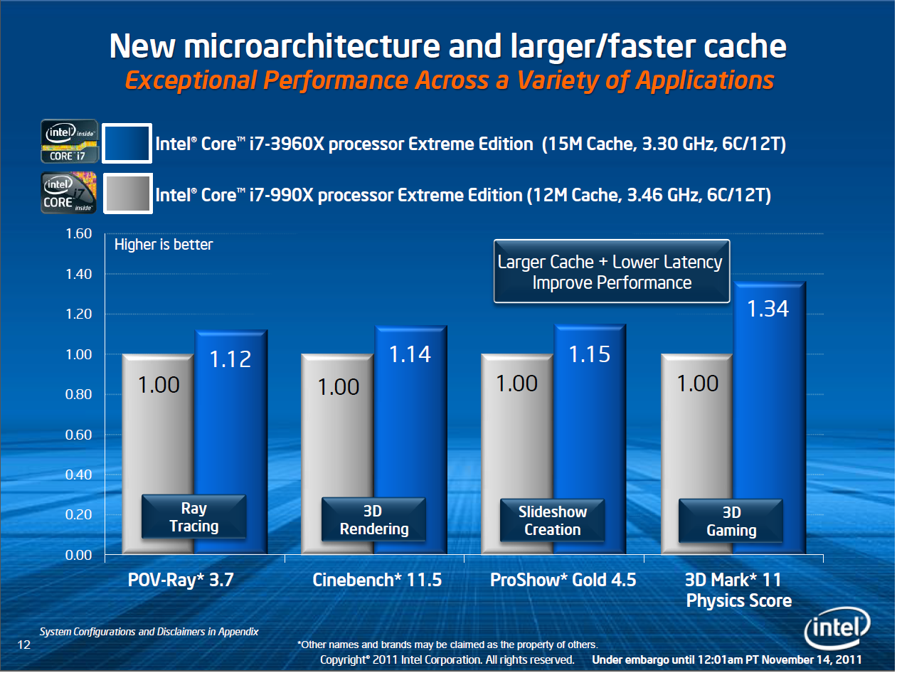
On Anand’s article regarding the CPUs, it is clear to say that anyone wanting performance can find it in Sandy Bridge-E. If you are willing to pay top dollar, you get a top CPU with six cores/twelve threads that will run between 3.6 GHz and 3.9 GHz (depending on CPU load) in a 130 W envelope. With a little push, this could easily see 4.5 to 4.7 GHz while on the Intel branded water cooler being sold separately. While this will not make much of a difference for gamers, we can see the allure for any CPU intensive tasks that are not already GPU accelerated – video encoding or rendering being obvious view points. The following is a slide from Intel’s press kit, comparing the performance of SNB-E i7-3960X to the i7-990X, where the main differences to X58 are the microarchitecture improvements (Nehalem->Sandy Bridge), the memory, and the larger cache:
Memory is a big part of X79, as we are introduced to quad channel memory on a mainstream consumer level chipset, compared to the previous enthusiast chipset, X58, where the push was in tri-channel memory. Most X79 boards will cater for 8 DIMM slots (2 DIMMs per channel), though some will scale this back to 4 DIMM slots to save money and space on the board. Theoretically, a 4x2 configuration will cater up to 64 GB of memory when using 8 GB memory sticks, though users will perhaps be looking in the $1600 range for such a kit (for example, Corsair’s Dominator 4x8 GB DDR3-1866 C9 kit CMT32GX3M4X1866C9) which surpasses the cost of a motherboard+CPU in one swoop. By specification, population of 8 DIMMs should make a motherboard default to 1333 C9 speeds, while when only using 4 DIMMs should give 1600 C9.
There are issues to the memory that a lot of people will consider – does anyone ever need 64 GB of memory? Even if it were populated with relatively cheaper 4 GB sticks, does anyone ever need 32 GB of memory? For the most part, no, however there is always a need for Virtual Machine memory, computational scientists requiring large data sets under a tighter budget, or animators requiring large rendering memory budgets. The flipside of the memory is that most motherboard manufacturers will support high memory frequencies – for example, as shown in the P9X79 PRO, up to DDR3 2666 MHz is selectable on the divider alone. In some pretesting, using a G.Skill RipjawsZ 4x4 GB kit, I have been able to hit 55 GB/s memory bandwidth quite happily. However, as stated previously, there are few users that this will be aimed at, but that is kind of the purpose of such a chipset.
There is argument here that Intel could have used dual channel memory for the high end – it would have reduced the pin count on the CPU (perhaps put it into an 1155 envelope, disregarding the PCIe connections) and ultimately the cost of the platform. Memory bandwidth is not a struggling feature for a lot of users, but those who found the memory bandwidth of X58 the limiting factor will enjoy the quad-channel of X79. Despite this, the specification does allow single, dual and tri-channel operation for X79, so it is completely possible that if micro-ATX or even mini-ITX motherboards are produced, they may scale back to two DIMM slots for dual channel operation. This gives a consumer up to 16 GB of memory, but should provide the same performance in non-memory bandwidth limited scenarios to Sandy Bridge based applications.
For the gamers and GPU users, we finally get full x16/x16 native compatibility in the PCIe world, without the need for any performance reducing NF200 solutions. X79 for the most part will see motherboards spouting x16/x16, x16/x16/x8, x16/x8/x8/x8, x8/x8/x8/x8 or even x16/x8/x8/x4/x4 variations depending on the PCIe layout of the board, the size of the board, and the manufacturer. For all intents and purposes, in gaming, we are not expecting this to make any difference for the first two GPUs. Very few gamers will be using more than two, and again, this chipset is aimed at ‘no price too much’ style scenarios. Where it will probably be handier is in the land of GPGPU, where CPU to GPU bandwidth may have been the major limitation in running simulations.
We cannot get away from the fact that for a lot of X79 motherboards, the PCIe GPU lanes will be post-specified at PCIe Gen 3. The chipset, and the motherboards in X79, should all display Gen 3 compatibility for the GPU slots (usually for the PCIe x8/x16), but this currently means relatively little for consumers until Gen 3 products are released to the market. There is also the fact that it cannot be properly tested in a real-world context until then – depending on how exactly the GPU manufacturers utilize the new technology. As a result, the initial batches of X79 motherboards may require a BIOS update to activate this functionality. I was lucky enough to observe an ASUS Z68 Gen 3 board running an Ivy Bridge processor at a recent invitational event, where ASUS were clearly stating that all their PCIe Gen 3 products are correctly implemented.
It is worth having a look at PCIe Gen 3, if only for a couple minutes. Inside the Intel Chipset implementation, it states:
Intel Core i7 and Intel Xeon processors in an LGA2011 package support PCI Express add-in graphics cards via the board’s PCI Express x16 connectors. These processors support the following generations of PCI Express:
- PCI Express 3.0 with a raw bit rate of 8.0 GT/s results in an effective bandwidth of 8.0 Gb/s each direction per lane. The maximum theoretical bandwidth of the x16 interface is 16 GB/s in each direction, simultaneously, for a bandwidth of 32 GB/s.
- PCI Express 2.x with a raw bit rate of 5.0 GT/s results in an effective bandwidth of 4.0 Gb/s each direction per lane. The maximum theoretical bandwidth of the x16 interface is 8 GB/s in each direction, simultaneously, for a bandwidth of 16 GB/s.
I want to draw attention to 3.0 and 2.x, and the comparison between GT/s (GigaTransfers per second) and bandwidth. It states, for 3.0, that there is a raw bit rate of 8.0 GT/s, and an effective up/down bandwidth total of 32 GB/s. For 2.x, there is a raw bit rate of 5.0 GT/s, and an effective up/down bandwidth total of 16 GB/s. This means there is a distinctive change in how PCIe 3.0 and 2.x operates – PCIe 2.0 uses an 8b/10b encoding scheme, which causes a 20% overhead; whereas PCIe 3.0 uses a ‘scrambling’ technology using binary polynomials and a 128b/130b encoding scheme, reducing overhead to 1.5%. So whereas PCIe 2.0 was a natural progression to PCIe 1.x, this is where the new 3.0 specific features are required in terms of processor and chipset.
The landscape of overclocking has also changed… slightly. The land of X58 overclocking was as varied as one could get – full multiplier and BCLK adjustable to get the balance a user wanted. Sandy Bridge and P67/Z68 changed all that, due to the internal clock generator, effectively being multiplier only. While this made overclocking easy for users and system builders alike, there were some outcries from various overclocking communities about ‘taking the fun’ out of overclocking. Sandy Bridge-E attempts to bridge the two systems with an overclocking hybrid of sorts. It all comes down to clock generators.
The initial CK505 clock generator, at 100 MHz, is split several ways – one to the CPU/memory, one to the PCIe, and one to the I/O. These splits act to gear the clock generator, allowing the user to adjust one without affecting the others. This opens up the CPU overclocking to a wider range of adjustments, rather than the 1-5 MHz sported on most Sandy Bridge/Cougar Point CPU and chipset combinations. A deeper look into how to overclock the Sandy Bridge-E platform is described later as part of the ASUS P9X79 Pro review. However, the broadside of SNB-E is that due to the design and the increased core count, it is expected that SNB-E processors may not overclock as well as Sandy Bridge for 24/7 use, leaving single core performance firmly in the hands of the mainstream processor market.
We are not afraid of overclocking 130W CPUs, despite the increased power draw and heat – a big feature of X58 was overclocking. However, while these SNB-E chips are also 130W, Intel is pushing the release of an Intel branded, all-in-one liquid cooler:
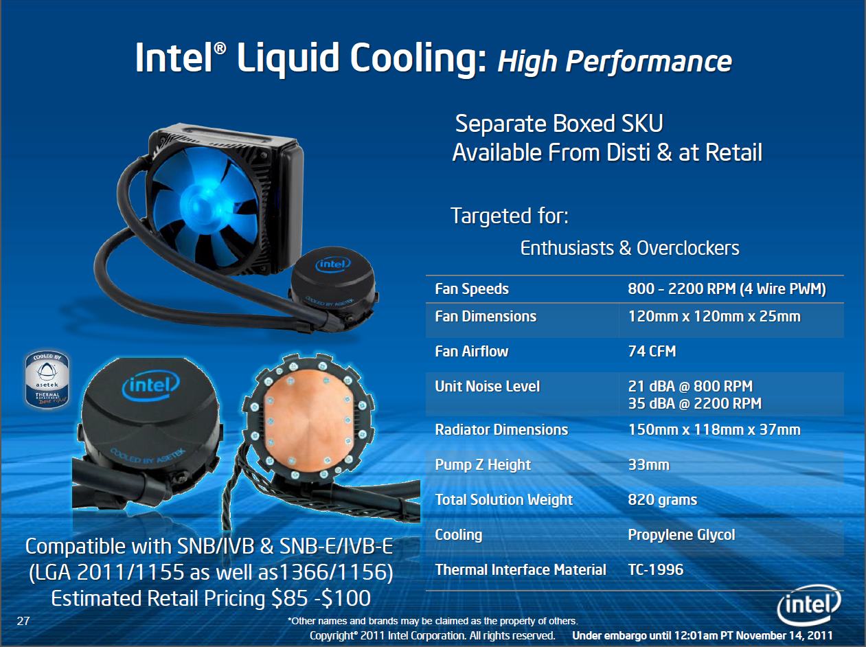
Made by Asetek, this is a simple 120mm single radiator cooler using propylene glycol whereby the fan plugs into a cable from the cooler, and the cooler plugs into the CPU fan header on the motherboard. This indicates that the pump and fan are both controlled by the onboard BIOS fan control implementation. In normal operation, using this cooler, I saw 61ºC in a forced 100% CPU load scenario (ambient 20ºC max) – in an overclocked (~30%) situation, this rose to 89ºC, where both liquid pipes to and from the cooler were warm. It’s not the most perfect water cooler on my brief analysis, but some substantial cooling will be required if users want an overclocked system. It also makes me wonder how Intel’s air cooler will fare, given that they suggest it is for stock systems only:

Lastly, we do lose a few features that have been on previous chipsets, or that were expected to be on X79. The most disappointing is perhaps the lack of USB 3.0 native to the chipset. It looks like we will have to wait until Ivy Bridge or even Haswell for updates on that end. Also, probably more of a carry over from P67/Z68, is that we still have a SATA 3 Gbps/SATA 6 Gbps discrepancy from the PCH. If AMD can stick 6 SATA 6 Gbps from their FCH implementations, it cannot be too much to ask for Intel to do it. It seems surprising then that we do not have Z68’s Smart Response Technology (SSD Caching) on X79 – though ASUS have devised a solution using a hardware/software combination which I will discuss later. Then there is the talk over SAS ports and compatibility – back at Computex when pre-release models of X79 boards were on show, they all had 6 SATA and 6 SAS ports on their models. But this was pulled from the specifications by Intel, for a variety of reasons. So while SNB-E and X79 are meant to be the pinnacle of performance and functionality, there is obviously still room for improvement if we literally want to have everything (no expense spared) in a chipset.
So, without further delay, let us rock on with one of the most important X79 motherboard releases – the ASUS P9X79 Pro!


55 Comments
View All Comments
buildingblock - Monday, November 14, 2011 - link
Amongst all the other goodies, the outstanding feature for me is the BIOS fan control. Well done to Asus, this board has probably the best PWM based fan control yet. Other board makers, particularly GigaByte, please take note.ASUSTechMKT - Monday, November 14, 2011 - link
Thanks so much for the feedback. We have been working hard to consistently improve in the quality of fan controls. Kudos to Ian for taking the time to detail it as well. This is somethign we have to take more time in the development ( Super I/O controller and frmware and software ) but any serious enthuiast can appreciate the additional functionality and increased usability.Thanks again!
jigglywiggly - Monday, November 14, 2011 - link
am i the only one kind of dissapointed? No integrated gpu is lame, also not that much faster.Kougar - Monday, November 14, 2011 - link
Holy moly, $330 for just the Pro?Given the extreme prices involved here, I'd especially like to know the key differences between the Pro and the Deluxe models, and even the Pro and the vanilla model as well.
ASUSTechMKT - Monday, November 14, 2011 - link
DeluxeOffers BT3.0 with Wifi, Additionally USB3, Dual Lan, A more advanced VRM heatsink assembly,
In regards to the pricing it is important to remember many of the additional items incorporated have a higher cost ( such as the hardware required to allow for UEFI flashing with CPU, Memory or a Graphics card this required a hardware level IC, the more advanced super I/O controller with more advanced fan controls for all the headers ) These additional touches add to the total cost of the board.
Kougar - Monday, November 14, 2011 - link
Thank you for the reply!For anyone else curious, after some digging I can say that in addition to the above, P9X79 Vanilla also loses the Marvell controller and associated SATA 6Gb/s ports. The Realtek sound chip also changes from a 898 to the 892, not sure what the difference is. The PWM phase design appears to remain unchanged between the vanilla and PRO models, while the Deluxe doubles the CPU & uncore phases.
Somewhat oddly, the P9X79 also gains a firewire port over the PRO model.
ASUSTechMKT - Wednesday, November 16, 2011 - link
Yes as you go up the boards you will also have more USB 3 (as the PRO has more USB which makes sense as 1394 is a legacy standard). Main reason it is offered on the Standard is that this model is adopted by sometimes business or professionals you still need some legacy connections.In regards to the overall VRM design we use the same high quality dual N mosfet package on all three boards and advanced driver this aligns with the high amperage rated choke. While the "phase" is increased on the Deluxe this only helps to slightly improve balancing of the VRM otherwise the performance for overall power delivery is rated the same. (Although the advanced heatsink design as you move up will help to ensure a cooler operating temperature for the VRM assembly.
Hope it helps!
Filiprino - Monday, November 14, 2011 - link
There was a rumour saying ASUS would release a dual socket LGA2011 motherboard to compete with EVGA SR-3. Any news?Kougar - Monday, November 14, 2011 - link
The board exists, but I haven't seen anything about it so far. Very curious to see it and the EVGA SR-3 compared, even if just to drool over!ASUSTechMKT - Wednesday, November 16, 2011 - link
Sorry cannot comment on that one......