AMD Announces Radeon RX 7800 XT & Radeon RX 7700 XT: Enthusiast-Class RDNA3 For 1440p Gaming
by Ryan Smith on August 25, 2023 11:30 AM EST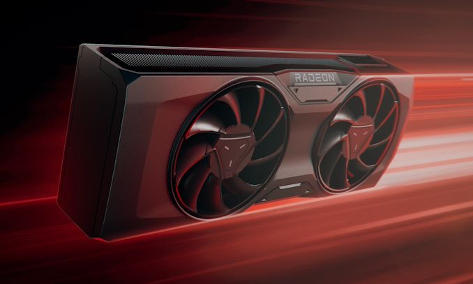
With the Gamescom convention taking place in Germany this week, AMD is using Europe’s largest video game trade show as the venue for their latest Radeon video card announcements. This morning the company is announcing their long-awaited middle members of the Radeon RX 7000 series, the Radeon RX 7800 XT and Radeon RX 7700 XT. Aimed at the 1440p gaming market and based on AMD’s new Navi 32 GPU, the new cards are designed to slot in to the middle of AMD’s product stack, offering a set of potent RDNA 3 architecture video cards for gamers who don’t need the bleeding-edge performance (and wallet-bleeding costs) of the Radeon RX 7900 series cards.
With today’s announcement being just that – an announcement – the retail launch of these cards, as well as AMD's new Hypr-RX enabled drivers, will follow in a couple of weeks, on Wednesday, September 6th. That date also not-so-coincidentally happens to be the release date for Bethesda’s ARPG Starfield, for which AMD is the game’s exclusive PC hardware partner, and which AMD will be offering with the new Radeon cards as part of the company’s latest game bundle. So for AMD, the stars are aligning to make September 6th a big day for the company’s GPU division.
But as for us, we’re here to talk about hardware, so let’s discuss the Radeon RX 7800 XT and 7700 XT, as well as the Navi 32 GPU that underpins them.
| AMD Radeon RX 7000 Series Specification Comparison | ||||||
| AMD Radeon RX 7800 XT | AMD Radeon RX 7700 XT | AMD Radeon RX 6800 XT | AMD Radeon RX 6700 XT | |||
| ALUs | 7680 (60 CUs) |
6912 (54 CUs) |
4608 (72 CUs) |
2560 (40 CUs) |
||
| ROPs | 96 | 96 | 128 | 64 | ||
| Game Clock | 2124MHz | 2171MHz | 2015MHz | 2424MHz | ||
| Boost Clock | 2430MHz | 2544MHz | 2250MHz | 2581MHz | ||
| Throughput (FP32) | 32.6 TFLOPS | 30 TFLOPS | 18.6 TFLOPS | 12.4 TFLOPS | ||
| Memory Clock | 19.5 Gbps GDDR6 | 18 Gbps GDDR6 | 16 Gbps GDDR6 | 16 Gbps GDDR6 | ||
| Memory Bus Width | 256-bit | 192-bit | 256-bit | 192-bit | ||
| Memory Bandwidth | 624GB/sec | 432GB/sec | 512GB/sec | 384GB/sec | ||
| VRAM | 16GB | 12GB | 16GB | 12GB | ||
| Infinity Cache | 64MB | 48MB | 128MB | 96MB | ||
| Total Board Power | 263W | 245W | 300W | 230W | ||
| Manufacturing Process | GCD: TSMC 5nm MCD: TSMC 6nm |
GCD: TSMC 5nm MCD: TSMC 6nm |
TSMC 7nm | TSMC 7nm | ||
| Transistor Count | GCD: ? MCD: 2B x4 |
GCD: ? MCD: 2B x4 |
26.8B | 17.2B | ||
| Architecture | RDNA3 | RDNA3 | RDNA2 | RDNA2 | ||
| GPU | Navi 32 | Navi 32 | Navi 21 | Navi 22 | ||
| Launch Date | 09/06/2023 | 09/06/2023 | 11/18/2020 | 03/18/2021 | ||
| Launch Price | $499 | $449 | $649 | $479 | ||
For this generation of video cards, AMD opted to eschew the usual top-to-bottom GPU and video card strategy in favor of releasing the top video cards (Radeon RX 7900 XTX & 7900 XT), and following that up with the bottom of the stack (Radeon RX 7600). As a result, this is one of those rare launches where the middle parts, broadly encompassing the “enthusiast” segment, are the final segment to launch. The precise order is generally immaterial, but it means we’re coming into the RX 7800 XT launch already knowing how the AMD cards above it and below it perform – and thus where it needs to be to best fit in to the product stack.
And with rival NVIDIA having already launched their complete stack of video cards for this generation, AMD also gets the advantage of knowing where to best position their cards against the competition. In this case, AMD is positioning the Radeon RX 7800 XT roughly against the GeForce RTX 4070, while its smaller sibling, the Radeon RX 7700 XT, will go up against the GeForce RTX 4060 Ti. NVIDIA has already shown their hand for 1440p gaming, so with this launch it’s up to AMD to decide how to best beat it.
Radeon RX 7800 XT & Radeon RX 7700 XT: By The Numbers
Leading things off is the Radeon RX 7800 XT, which AMD will be positioning as their premiere 1440p gaming card. The RX 7800 XT has a near-full Navi 32 configuration (more later) with 60 CUs integrated, affording 7680 ALUs (3840 stream processors). AMD is clocking this part a little less aggressively than what we’ve seen with the flagship RX 7900 XTX, giving us a peak boost clock of 2430MHz and an average game clock of 2124MHz. On paper this gives the card an average FP32 compute throughput of 32.6 TFLOPS, though as has been the case with the rest of the RDNA 3 family, the architectural changes make throughput comparisons against prior AMD cards tricky.
By the numbers, the RX 7800 XT offers about 76% of the compute throughput of the next card up, the RX 7900 XT. Notably, however, the number of ROPs has been halved versus both RX 7900 series cards, so the actual rendered pixel throughput is closer to 50%. Few games are entirely ROP-bound, so the actual performance gap between this card and the 7900 XT shouldn’t be nearly as big, but it underscores the fact that we’re not looking at something as straightforward as 75% of a 7900 XT.
With 4 active MCDs, the RX 7800 XT is attached to a 256-bit GDDR6 memory bus. While we’ve seen the 7900 series cards clocked at 20Gbps, AMD has taken the odd choice to dial down the clocks on the 7800 XT just a bit, to the noticeably fractional 19.5Gbps. This gives the resulting card a total of 624GB/second of memory bandwidth. That, in turn, is further augmented with 64MB of Infinity Cache spread among the MCDs, two-thirds of the cache found on AMD’s flagship cards.
The use of a 256-bit memory bus means that AMD is easily able to equip the card with 16GB of VRAM, which is going to be a major marketing point from the company in competing with the GeForce RTX 4070 and its 12GB of VRAM sitting on a 192-bit memory bus. Consequently, AMD has the edge in both memory capacity and memory bandwidth, though as we’ve seen in the past, that won’t necessarily translate into a performance advantage for AMD.
Meanwhile, with the overall design of Navi 32 favoring cost over power efficiency, the power consumption of the 7800 XT is going to run at a relatively high 263 Watts, 37W less than the 7900 XT. AMD is not going to be able to win the power efficiency race with NVIDIA here (and arguably they never even intended to try) so instead the RX 7800 XT is configured to maximize its performance. Note that these are AMD’s baseline specifications, and factory overclocked AIB partner cards can go higher.
Making generational comparisons here is a bit tricky, both due to the architectural changes from RDNA 2 to RDNA 3, as well as some quirks in AMD’s own card positioning for this generation. While the RX 7800 XT is AMD’s 3rd/4th tier card overall (behind the three 7900 series cards), its direct predecessor, the RX 6800 XT, was AMD’s second-tier card, behind only the flagship 6900 XT. Long story short, the 6800 XT/7800 XT comparison isn’t especially flattering for AMD – the number of CUs has gone down by a bit – though so has power consumption and price. The more apt comparison is arguably the RX 6800 vanilla, but I digress.
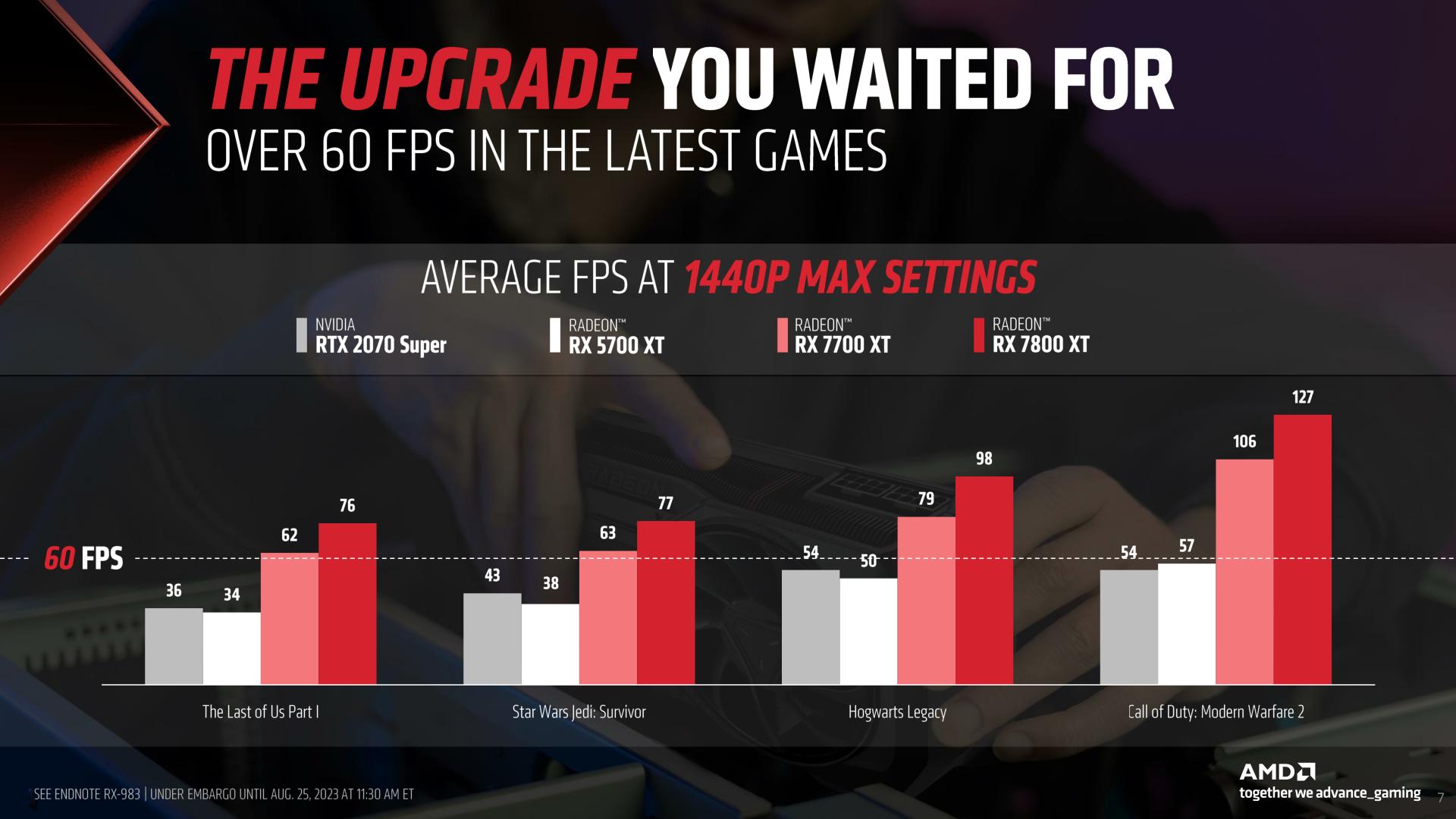
In any case, the big generational upgrade push from AMD is going to be pitting the RX 7800 XT against cards that are now coming up on four years old, such as the Radeon RX 5700 XT and GeForce RTX 2070. The RX 7800 XT should roughly double the performance of those cards, making them a more palatable upgrade for system owners whose current 1440p cards are no longer keeping up.
Sapphire Pulse RX 7700 XT
Finally, standing in line behind the RX 7800 XT, we have the RX 7700 XT. This is a cut-down Navi 32-based card that, despite the lower series number, is also aimed at 1440p gaming.
Hardware-wise, we’re looking at 54 CUs, with a maximum boost clock of 2544MHz and an average game clock of 2171MHz. As a result, the compute performance of the RX 7700 XT is, on paper, quite close to its bigger brother, with the smaller card slated to deliver 92% of the RX 7800 XT’s compute performance. And, notably, there is no cut to the number of ROPs here, so the overall pixel pushing power is technically ever so slightly in the RX 7700 XT’s favor.
Instead, what will be driving the bulk of the performance differences between the two cards will be memory bandwidth. The RX 7700 XT only features 3 active MCDs (like the 7900 XT, the inactive MCD is kept as a dummy spacer), which means it’s losing a quarter of its memory bus, as well as a quarter of its Infinity Cache. Coupled with that, AMD has cut the memory clocks a bit more, bringing them down to 18Gbps/pin. The net result is that the RX 7700 XT offers 69% of the RX 7800 XT’s memory bandwidth, and 75% (48MB) of the Infinity Cache capacity. All of which means that it will be just how memory and cache bandwidth-bound a given game is that determines how close the RX 7700 XT can get to the RX 7800 XT.
The smaller memory bus also means that the card comes with less VRAM overall. In this case, we’re looking at 12GB of GDDR6. With AMD positioning this card against NVIDIA’s 128-bit GeForce RTX 4060 Ti, that means they have a memory capacity and bandwidth against the baseline 8GB model, though NVIDIA’s partners are also offering a 16GB model that leaves the RX 7700 XT smack dab in the middle.
Otherwise, with clockspeeds running even higher than the RX 7800 XT, the RX 7700 XT picks up very little in power savings. AMD has the card’s official TBP at 245W, just 18W less than the RX 7800 XT. Assuming what real-world power consumption matches this figure (which is not always the case), then it means that the RX 7700 XT is going to be less power efficient of the two cards overall. And, for that matter, far less power efficient than NVIDIA’s 160W RTX 4060 Ti.
The RX 7700 XT will be replacing the RX 6700 XT within AMD’s product stack, which at the time of its introduction, was the top Navi 22 card. While we don’t have any comparative performance figures, the RX 7700 XT overall enjoys a 35% bump in CU count, albeit at a ~10% regression in average clockspeeds. All the while power consumption has trickled up a bit from 230W. So it should make for a modest generational jump over its direct predecessor.
Navi 32: A Second, Smaller Chiplet GPU
Driving both cards is AMD’s new RDNA 3 architecture-based Navi 32 GPU. This is the second consumer chiplet GPU from the company, and is essentially a smaller take on Navi 31 that powers the RX 7900 series. In this case “smaller take” means that AMD is using a new Graphics Compute Die (GCD) with fewer functional blocks and transistors, trading off performance for lower power consumption and manufacturing costs. Meanwhile the GCD is being paired with 4 of AMD’s Memory Cache Dies (MCD), which are being reused from Navi 31.
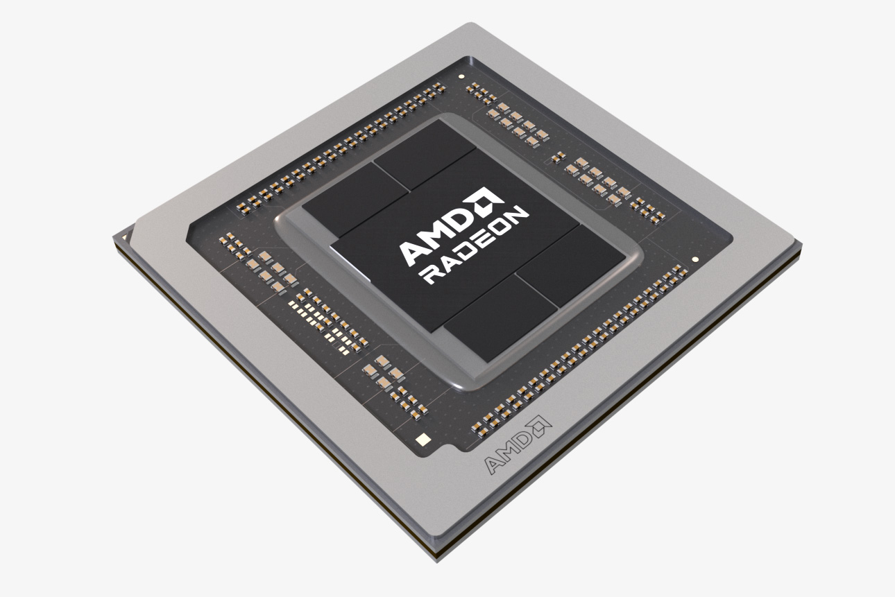
As with Navi 31, the intricate GCD is fabbed on TSMC’s 5nm process, building the scalable and performance critical parts of the GPU on a leading-edge TSMC process. Meanwhile the MCDs continue to be produced on TMSC’s 6nm process, housing parts of the GPU that don’t scale well with smaller nodes, such as the Infinity Cache and GDDR6 memory controllers. So Navi 32 is a mix of new and old(er) process nodes with regards to its fabrication, while it’s on the cutting edge of packaging.
Broadly speaking, the entire Navi 3x GPU lineup is designed to be cost-efficient from a manufacturing standpoint, and Navi 32 is no different. AMD is only producing the critical bits on a leading edge 5nm node – and even then, not using TSMC’s bleeding-edge 4nm variant – while producing the rest on a cheaper 6nm node. Without going too far down the rabbit hole for this announcement, this has performance implications that become a factor in how AMD configures and positions their cards. But at a high level, the takeaway is that the novelty of a chiplet-based GPU aside, Navi 32 follows a notably different design strategy than past enthusiast-class AMD GPUs, or for that matter rival NVIDIA’s monolithic designs. As we’ve seen with the RX 7900 series, this is going to be the most noticeable in power consumption, and is likely the biggest factor in why both Navi 32 cards have TBP specs well above their NVIDIA competition.
For now, we’re still waiting on AMD to confirm some of the specifications of Navi 32, in particular the die size of the GCD and its transistor count. Based on AMD’s off-angle die photo, we’re currently estimating a rough 211mm2 based on the known size of the MCDs (37.5mm2), but that’s a rough guess at best. That would put it at around two-thirds the size of the Navi 31 GCD.
At this point we’re also awaiting confirmation on the total number of CUs available within the GPU. While the RX 7800 XT is the top tier part, AMD has not confirmed whether Navi 32 itself also only has 60 CUs, or if it has more. Given that Navi 31 was 96 CUs and Navi 33 was 32 CUs, it’s likely that Navi 32 is a 64 CU design, but stranger things have happened.
Otherwise, Navi 32 is RDNA 3 through and through. This means it incorporates the same architectural changes we’ve seen in the rest of the RX 7000 series lineup, such as AV1 encode/decode support, improved ray tracing performance, AMD’s new DisplayPort UHBR13.5-capable Radiance display controller, and the second bank of ALUs for dual-issuing suitable instructions and improving AI performance.
Reference Cards, Partner Cards, & Product Positioning
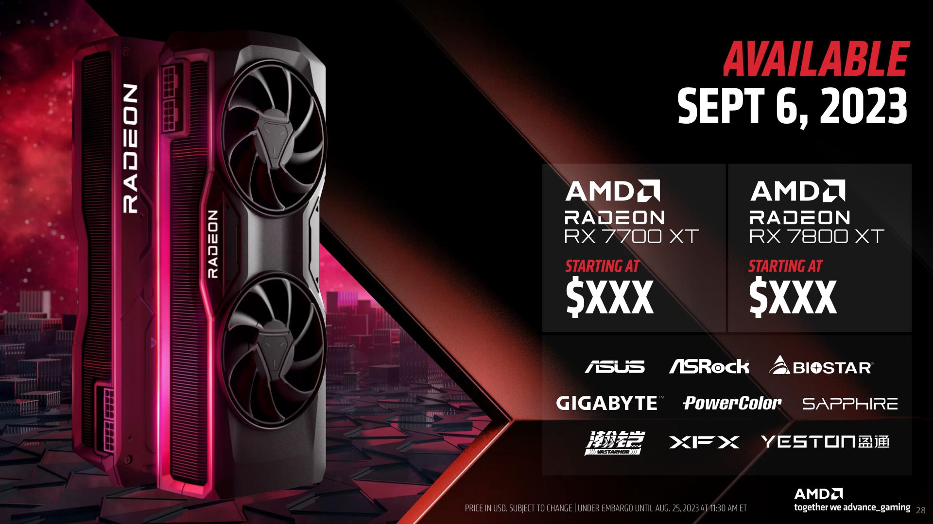
As noted earlier, both cards will be launching in a couple of weeks, on September 6th. With regards to reference cards, AMD is essentially splitting the difference – they will be selling a reference Radeon RX 7800 XT through their website, but not a reference Radeon RX 7700 XT. Instead, AMD’s board partners will be swooping in to support the launch of both cards, with AIB designs slated to be available for both cards on the launch day.
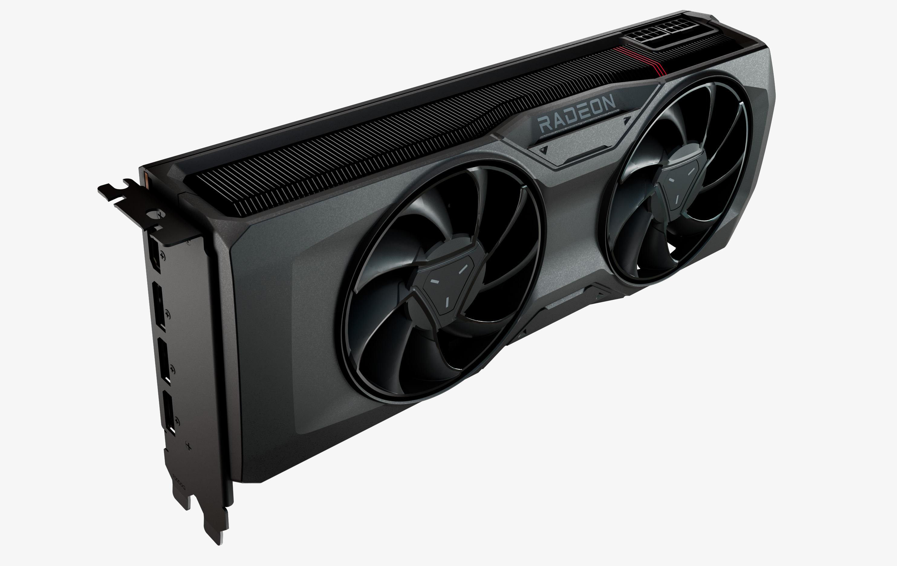
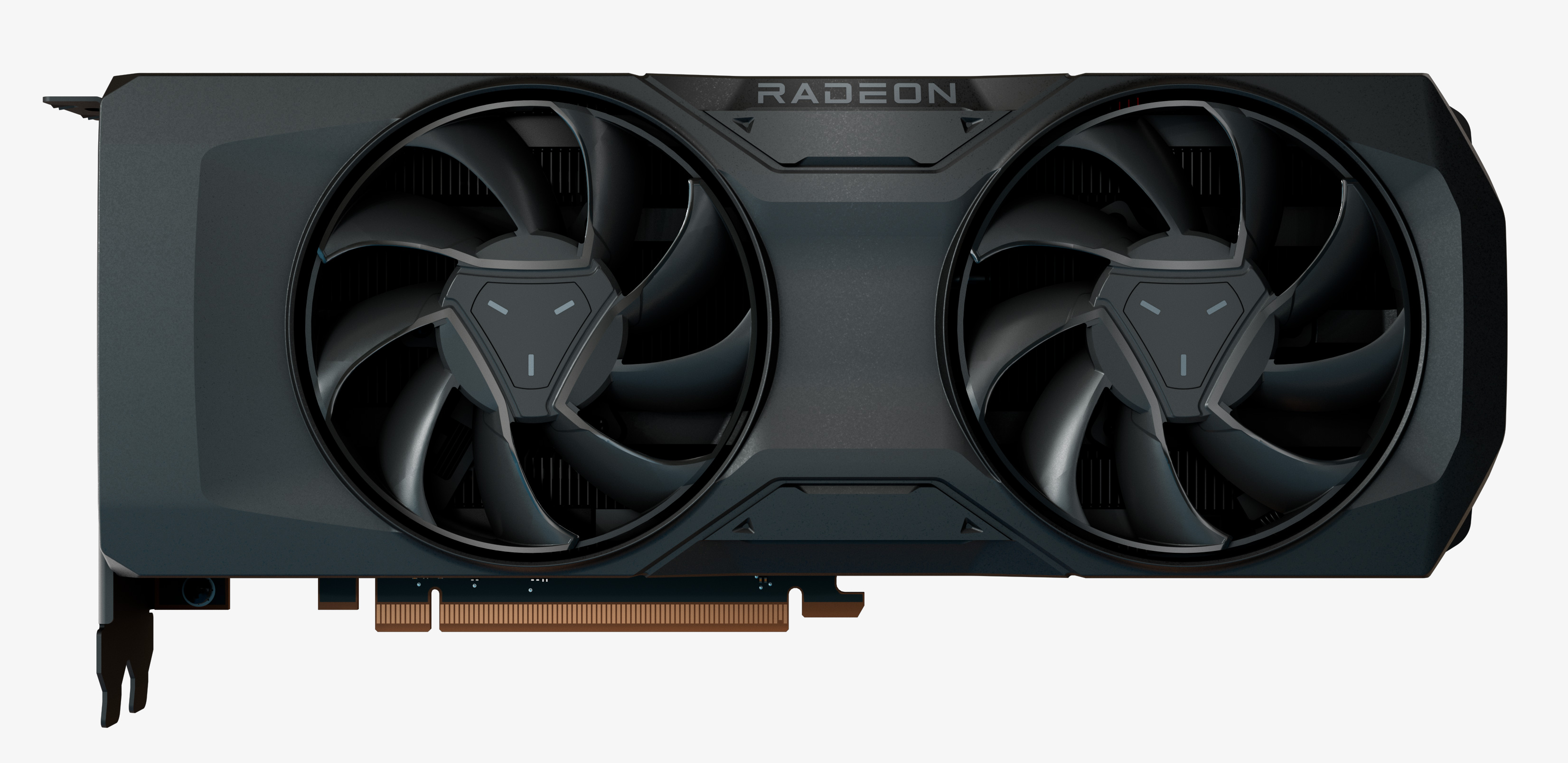
Taking a brief look at AMD’s reference card, it’s a fairly sizable twin-fan open air design, copying the design aesthetics from AMD’s reference RX 7900 series cards. At two fans it’s smaller overall, but not immensely so. Notably, this is a 2.5 slot card, which not all of the pictures show very well, so it will need some extra room to breathe.
Powering the card is a pair of 8-pin PCIe power sockets. Strictly speaking, this is technically overkill, since a 6+8 configuration would still be good for 300W. But more and more we’re seeing 6-pin sockets go away entirely, so it’s not entirely surprising to see AMD go for 8+8. As noted earlier, the TDP of the reference card is 265W, however AIB partners can (and will) clock some of their cards higher with higher TDPs to match.
Meanwhile, AMD’s port configuration has taken a bit of a departure from the RX 7900 reference designs. While still offering 4 ports, AMD has thrown out the USB-C port in favor of another full-size DisplayPort. The result is a trio of DisplayPorts that support DP 2.1 at data rates of up to UHBR13.5, as well as a sole HDMI port supporting HDMI 2.1.
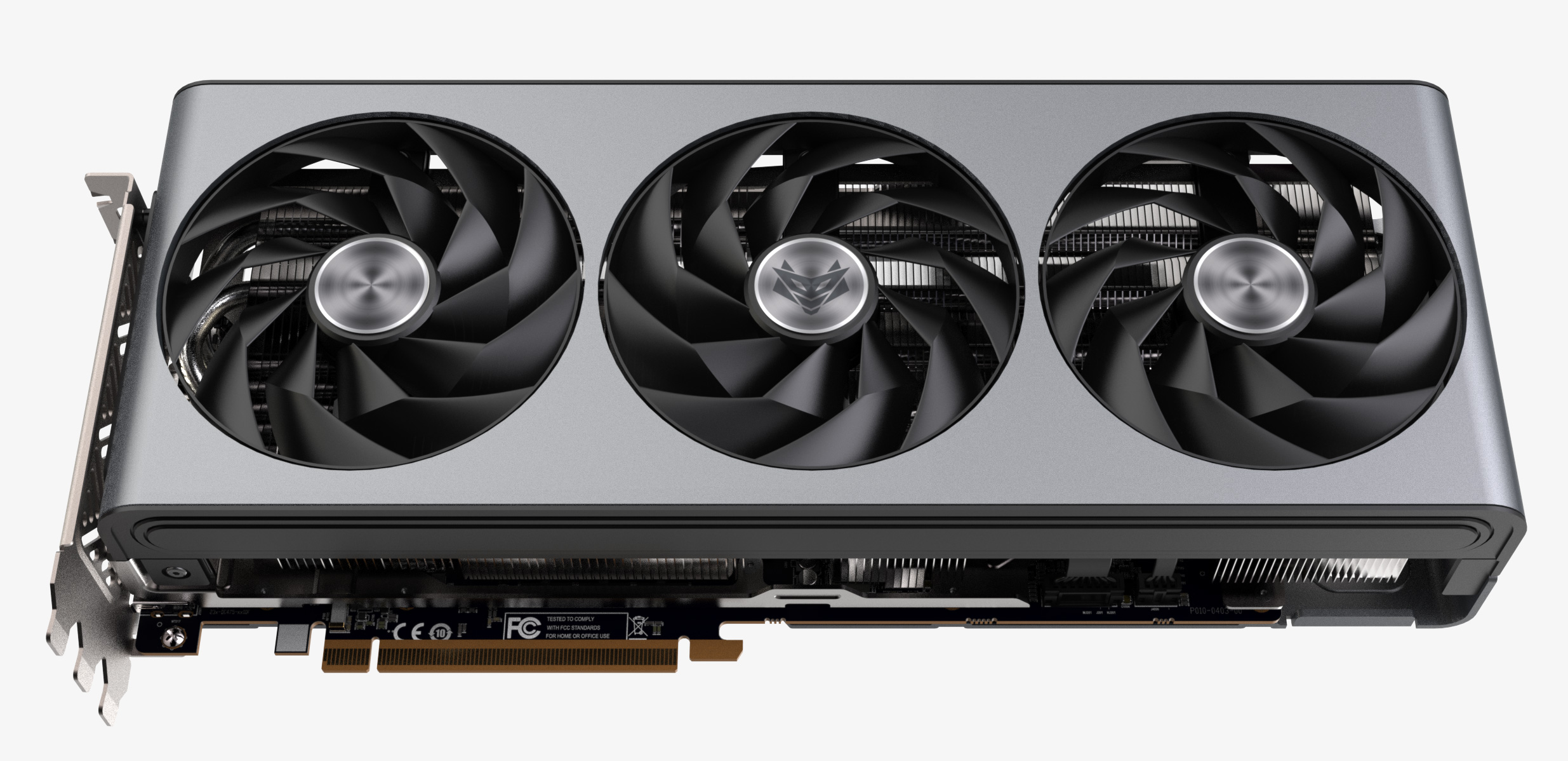
Sapphire's Nitro RX 7800 XT & RX 7700 XT
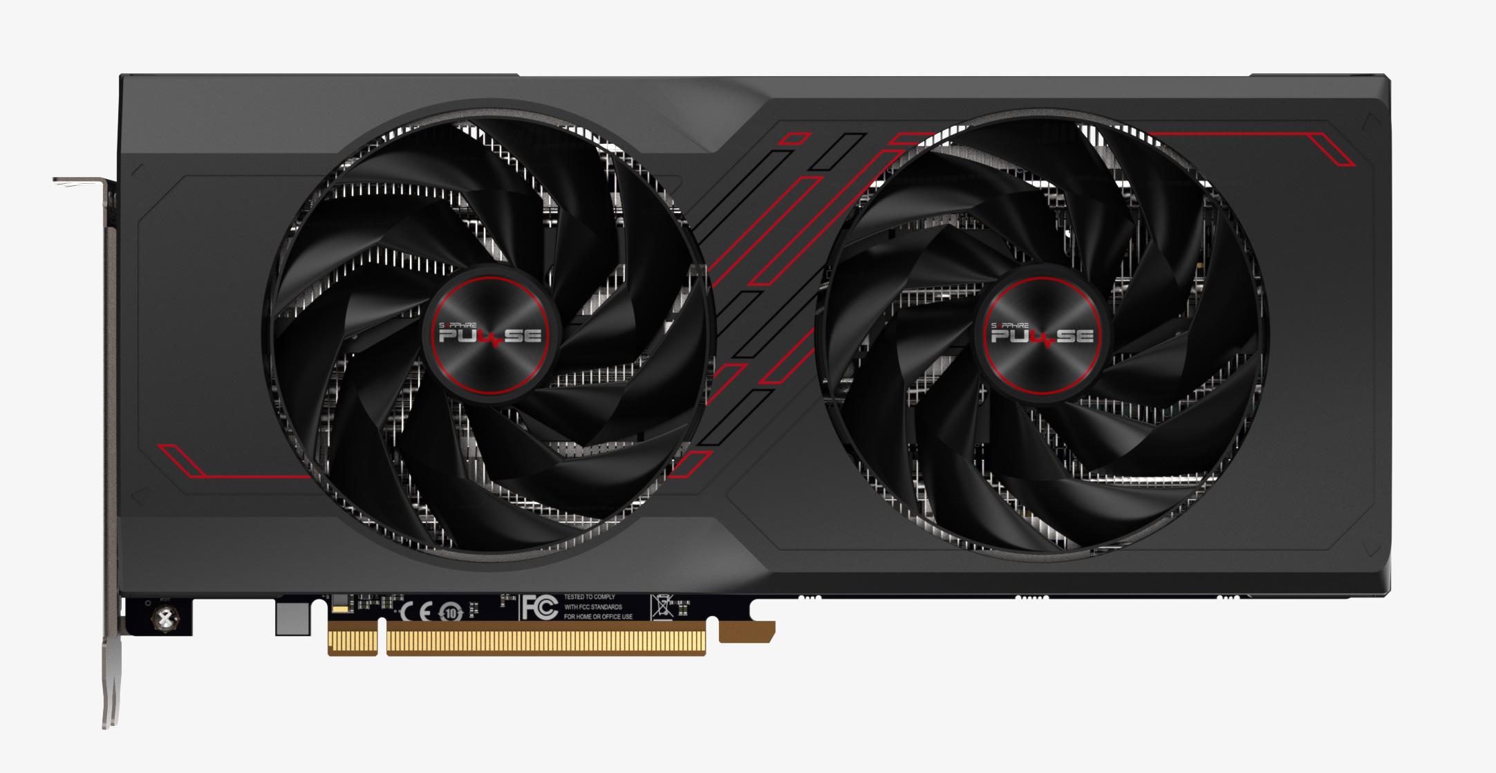
As for the partner cards, all of the usual suspects have RX 7800/7700 designs in the works, including ASUS, GIGABYTE, Sapphire, PowerColor, and more. AMD sent over a couple of dozen photos showing off the different designs, a lot of which are triple-fan cards that look like their existing RX 7900 designs.


Unfortunately, most of these photos are head-on shots, so we can’t tell whether many (if any) are true dual-slot designs (versus the 2.5 slot design of the AMD reference card). Due to the relatively high TBPs, the RX 7800/7700 series puts AMD and its partners in a bit of a tough place when it comes to producing SFF-sized cards. We’ll have more information once the board partners post their official product pages, but at first blush, it doesn’t look like we’ll see much in the way of small cards – at least initially.
In terms of competition, AMD is setting up the RX 7800 XT and RX 7700 XT roughly against the GeForce RTX 4070 and GeForce RTX 4060 Ti respectively – with AMD believing they’re in the lead, of course. It’s a bit of an odd match-up since the RTX 4060 Ti is not primarily aimed at 1440p gaming the way the RX 7700 XT is, but this is hardly the first time AMD and NVIDIA’s cards don’t perfectly line up.
Just how well they compare, however, remains to be seen. Not just for independent performance benchmarks, but because AMD is not disclosing the price of either card to the press ahead of time. So whether AMD is going for iso-pricing or if they intend to undercut NVIDIA in some fashion remains to be seen.
Update: Now that the official announcement has gone out, AMD has disclosed the price of the cards. The Radeon RX 7800 XT will start at $499, while the Radeon RX 7700 XT will start at $449. The rest of the original article follows as below.
But, in a sign that AMD likely isn’t going to be too aggressive on pricing, the company is extending their current Starfield promotional game bundle to cover the new Radeon cards; so both the RX 7800 XT and RX 7700 XT will be coming with a game bundle right off the bat. Starfield is AMD’s big game partnership for the year, so the company is keen to promote what they see as one of the most important games of the year. At the same time, game bundles are traditionally used to prop up video card prices in lieu of price cuts by adding value to the overall package.

Ultimately, just how successful the Radeon RX 7800 XT and RX 7700 XT are will be entirely in AMD’s hands. RDNA 3 is a solid architecture, and thanks to the company’s cost-optimized chiplet-based design strategy, they shouldn’t have any trouble hitting price points that make both cards competitive. The only real question is just how many cards AMD wants to sell – and thus what price points they target.
Wrapping things up, the Radeon RX 7800 XT and RX 7700 XT will be launching on September 6th. AMD will be carrying their reference RX 7800 XT directly on their website, meanwhile Newegg, Amazon, and other retailers and etailers will be carrying the various AIB cards that the partners have put together.


| Q3 2023 GPU Product Lineups (Approximate MSRPs) |
|||||
| AMD | Price | NVIDIA | |||
| $1599 | GeForce RTX 4090 | ||||
| $1199 | GeForce RTX 4080 | ||||
| Radeon RX 7900 XTX | $999 | ||||
| Radeon RX 7900 XT | $799 | GeForce RTX 4070 Ti | |||
| $599 | GeForce RTX 4070 | ||||
| Radeon RX 7800 XT | $499 | GeForce RTX 4060 Ti (16GB) | |||
| Radeon RX 7700 XT | $449 | ||||
| $399 | GeForce RTX 4060 Ti (8GB) | ||||
| $299 | GeForce RTX 4060 | ||||
| Radeon RX 7600 | $269 | ||||


38 Comments
View All Comments
brucethemoose - Friday, August 25, 2023 - link
I really like that MCD-GCD split.AMD can fab those small memory controller/cache chips cheaply, on a density optimized process. The cache chips don't care about being split up, as memory access is interleaved anyway, hence there is no communication between memory dies.
And the compute die can focus soley on compute, without wasting tons of die area on pins for the GDDRX or last level cache.
The scheme saves tape out costs, as the memory die is reused across the stack and the compute die can be relatively small.
But I wonder why AMD didn't make a 512-bit GPU with a 600mm^2+ compute die. They could have killed the 4090 with this architecture, and they could sell a 64GB version as a cheap server inference card... But they chose not to.
meacupla - Friday, August 25, 2023 - link
They are probably focusing their efforts on RDNA 4 and Navi 4C.brucethemoose - Friday, August 25, 2023 - link
It probably wouldn't stress AMD's engineers too much? They would tape out a compute die and test the package, but the memory dies and the basic architecture are already worked out.This is all hypothetical though, as its indeed too late to start a new RDNA3 product.
Zoolook - Saturday, August 26, 2023 - link
There is a relatively long lag from when the configuration decisions are made and when the product is released, with most parameters unknown to us. Process availability etc.Most likely if they had the knowledge about available today they would have made different choices back then. Sure there are minor configuration choices made after the chips are ready, like frequencies, memory speed etc, but those are minor adjustments within the possibilities given by the hardware.
It's very complex guesswork.
Bruzzone - Friday, August 25, 2023 - link
Bruce, what do you think the memory latency is between, on and off, back and forth between GCD and MCD? SIP interconnect has to through Serdes is that not correct? mbBruzzone - Friday, August 25, 2023 - link
I also wonder if there are third party memory suppliers, standard products, qualified for the memory components? Price competitive supply. mbmode_13h - Saturday, August 26, 2023 - link
> what do you think the memory latency is between, on and off, back and forth between GCD and MCD?Maybe AMD mentioned this in the original RDNA3 architecture slide deck, or at Hot Chips? I know they provided bandwidth numbers.
For me, the big question is how the cache on the MCDs functions. I wonder if it's tied to the address range of the DRAM attached to the MCD, or if it's in a global pool? It matters a lot, especially with RDNA3 having less L3 cache than RDNA2 had. If it's being subdivided by address range, then the effect is that you have even less.
brucethemoose - Saturday, August 26, 2023 - link
Subdividing them by address range seems very inefficient. The memory chips and controllers are already interleaved, so the cache mind as well be interleaved too, right?mode_13h - Saturday, August 26, 2023 - link
Do you know, for a fact, that these GPUs interleave memory accesses? I wouldn't assume so.And, what I meant by "subdividing by address range" was essentially having the cache front whatever DRAM is attached to the MCD. I wasn't suggesting there'd be a partitioning scheme different than the memory. Either it's partitioned according to how the attached memory is partitioned, or it's global. Those are the only two realistic possibilities. I just wonder which.
brucethemoose - Saturday, August 26, 2023 - link
I have no clue, and I haven't seen it mentioned anywhere. It would be interesting to know... Maybe a chipsandcheese cache benchmark will coax it out?