E3 2005 - Day 2: More Details Emerge on Console GPUs
by Anand Lal Shimpi on May 19, 2005 1:24 PM EST- Posted in
- Trade Shows
Scratching the Surface of NVIDIA's RSX
As we mentioned before, NVIDIA's RSX is the more PC-like of the two GPU solutions. Unlike ATI's offering, the RSX is based on a NVIDIA GPU, the upcoming G70 (the successor to the GeForce 6).
The RSX is a 90nm GPU weighing in at over 300 million transistors and fabbed by Sony at two plants, their Nagasaki plant and their joint fab with Toshiba.
The RSX follows a more conventional dataflow, with discrete pixel and vertex shader units. Sony has yet to announce the exact number of pixel and vertex shader units, potentially because that number may change as time goes by depending on yields. This time around Sony seems to be very careful not to let too many specs out that are subject to change to avoid any sort of backlash as they did back with the PS2. Given the transistor count and 90nm process, you can definitely expect the RSX to feature more than the 16 pipes of the present day GeForce 6800 Ultra. As for how many, we'll have to wait for Sony on that.
NVIDIA confirmed that the RSX is features full FP32 support, like the current generation GeForce 6 as well as ATI's Xbox 360 GPU. NVIDIA did announce that the RSX would be able to execute 136 shader operations per cycle, a number that is greater than ATI's announced 96 shader ops per cycle. Given that we don't know anything more about where NVIDIA derived this value from, we can't be certain if we are able to make a direct comparison to ATI's 96 shader ops per cycle.
Given that the RSX is based off of NVIDIA's G70 architecture, you can expect to have a similar feature set later this year on the PC. In fact, NVIDIA stated that by the time PS3 ships there will be a more powerful GPU available on the desktop. This is in stark contrast to ATI's stance that a number of the features of the Xbox 360 GPU won't make it to the desktop for a matter of years (potentially unified shader architecture), while others will never be seen on the desktop (embedded DRAM?).
There will definitely be some differences between the RSX GPU and future PC GPUs, for a couple of reasons:
1) NVIDIA stated that they had never had as powerful a CPU as Cell, and thus the RSX GPU has to be able to swallow a much larger command stream than any of the PC GPUs as current generation CPUs are pretty bad at keeping the GPU fed.
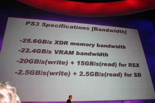
2) The RSX GPU has a 35GB/s link to the CPU, much greater than any desktop GPU, and thus the turbo cache architecture needs to be reworked quite a bit for the console GPU to take better advantage of the plethora of bandwidth. Functional unit latencies must be adjusted, buffer sizes have to be changed, etc...
We did ask NVIDIA about technology like unified shader model or embedded DRAM. Their stance continues to be that at every GPU generation they design and test features like unified shader model, embedded DRAM, RDRAM, tiling rendering architectures, etc... and evaluate their usefulness. They have apparently done a unified shader model design and the performance just didn't make sense for their architecture.
NVIDIA isn't saying that a unified shader architecture doesn't make sense, but at this point in time, for NVIDIA GPUs, it isn't the best call. From NVIDIA's standpoint, a unified shader architecture offers higher peak performance (e.g. all pixel instructions, or all vertex instructions) but getting good performance in more balanced scenarios is more difficult. The other issue is that the instruction mix for pixel and vertex shaders are very different, so the optimal functional units required for each are going to be different. The final issue is that a unified shader architecture, from NVIDIA's standpoint, requires a much more complex design, which will in turn increase die area.
NVIDIA stated that they will eventually do a unified shader GPU, but before then there are a number of other GPU enhancements that they are looking to implement. Potentially things like a programmable ROP, programmable rasterization, programmable texturing, etc...
Final Words
We're going to keep digging on both of these GPUs, as soon as we have more information we'll be reporting it but for now it's looking like this is the best we'll get out of Microsoft and Sony.


22 Comments
View All Comments
finbarqs - Saturday, May 21, 2005 - link
perhaps that's why they were very *hush* *hush* regarding their PS3 GPU. For all we know, the Sony demo's is very possible on the XGPUIllissius - Saturday, May 21, 2005 - link
It'd have been nice to have some specs for current desktop GPUs in there for comparison purposes... how many shader ops/sec can they do? 16 + 6 = 22?ksherman - Saturday, May 21, 2005 - link
DAmn they cant count! they just explained what the transisters are doing, and last i checked 232million+100million != 232million!Low Roller - Saturday, May 21, 2005 - link
IGN posted an update to their Xbox 360 specs:"Lastly, we were sent updated spec numbers on the Xbox's numbers, and we spoke with Microsoft's Vice President of hardware, Todd Holmdahl, about the Xbox 360's final transistor count.
Another bit of information sent our way is the final transistor count for Xbox 360's graphics subset. The GPU totals 332 million transistors, which is spit between the two separate dies that make up the part. The parent die is the "main" piece of the GPU, handling the large bulk of the graphics rendering, and is comprised of 232 million transistors. The daughter die contains the system's 10MB of embedded DRAM and its logic chip, which is capable of some additional 3D math. The daughter die totals an even 100 million transistors, bringing the total transistor count for the GPU to 232 million."
http://xbox360.ign.com/articles/617/617951p3.html
Low Roller - Friday, May 20, 2005 - link
OK, I did a bit more hunting around on the transistor count in the Xbox 360's GPU, and the only thing I've found comes from Microsoft's Major Nelson.(Xbox Live Director of Programming)According to his blog, the Xbox 360's GPU has 330 million transistors.
http://www.majornelson.com/2005/05/20/xbox-360-vs-...
I'm not sure how credible either IGN's or Major Nelson's figures are on this, as their not even close to each other.
ksherman - Friday, May 20, 2005 - link
WOAAA, so Sony is manufacturing nVidia's GPU? really weird.. hope sony got a discount on the price of the core then...Calin - Friday, May 20, 2005 - link
Just remember that video chipsets developers have multiple teams working on different generations - they have one chip in early development and one in late development/near production. This means two teams at least (to keep up with the 6 month product launches that were the norm starting from some 3 years ago)Cygni - Friday, May 20, 2005 - link
With the memory controller functions ALSO on the 360 GPU, 150 million is pretty darn out of reach, im thinking. The 360 GPU almost sounds like an integrated single chip north bridge. It will be interesting to crack an Xbox360 open and get a peak at the insides when it ships. Should be interesting.I couldnt help but wonder if perhaps this is a tile based arch... any info on that? If so, it would answer a few of my questions about the system.
Anand Lal Shimpi - Friday, May 20, 2005 - link
Low RollerJarred is correct, the IGN figures have to be wrong. Remember that R420, a 16 pipe design, was already around 160M transistors. The Xbox 360 GPU has 48 pipes, although they are unified shader pipes. Add in the additional logic to deal with handling both vertex and pixel instruction streams and you are already dealing with a GPU that is larger than the R420.
Not to mention the 10MB of embedded DRAM, which will not be tiny.
Take care,
Anand
IceWindius - Friday, May 20, 2005 - link
I think im gonna give up on the upgrade race for PC's, im so tired of it. Think i'll go buy Xbox360, PS3 and come out money ahead.