FIC VA-503+ MVP3 Super7 Board
by Anand Lal Shimpi on June 9, 1998 2:08 PM EST- Posted in
- Motherboards
Anand Tech Report Card Rating
90/B+
| CPU Interface | Socket-7 |
| Chipset | VIA MVP3 |
| L2 Cache | 512/1024KB |
| Form Factor | AT |
| Bus Speeds | 66 / 75 / 83 / 90 / 100 / 112 MHz |
| Clock Multipliers | 1.5x - 5.5x |
| Voltages Supported | 2.0v - 3.3v (in 0.1v steppings) |
| Memory Slots | 2 168pin DIMM Slots
(EDO/SDRAM) 4 72pin SIMM Slots (EDO/FPM) |
| Expansion Slots | 1 AGP Slot 3 PCI Slots (1 Full Length) 3 ISA Slots (1 Shared / 2 Full Length) |
| BIOS | AWARD PnP BIOS |
| Like Shuttle's HOT-591P, the FIC VA-503+ gives new meaning to the title "Baby AT Form Factor" as the board measures in just under a 9" x 9" square, the decrease in PCB size (Printed Circuit Board) is reflected greatly in the $106 price of the board which should definitely be a plus for those on a tight budget yet looking for the most bang for their buck. Unlike Shuttle's MVP3 board however, the VA-503+ allows for a single PCI slot to be populated by a full length PCI card. The last of three PCI slots just barely clears the CPU Socket by about a centimeter allowing for a Voodoo2 accelerator or other full length PCI card to be installed. On the opposite end the first two of the three ISA slots on the VA-503+ can accept full length cards, while the third slot falls in the path of the CPU Socket making a full length card a no-go in the last ISA slot. The memory expansion slots on the VA-503+ are reminiscent of those found on the old Intel TX based FIC PT-2007 as they come in the original 4 SIMM + 2 DIMM combination. Provided you have some decent quality 60ns or faster EDO SIMMs laying around, those 4 SIMM slots won't go to waste as the MVP3 chipset found on the board will enable you to lock the Memory Bus (the speed at which your memory operates at) at or around the 66MHz marker, even if the Front Side Bus (FSB - speed from which your CPU/L2 cache derive their clock speeds) is running at 100MHz. | 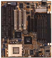 |
The VA-503+ fully supports a wide variety of FSB Speeds and Core Voltages to cover virtually all possible standard and overclocked settings you may wish to run your processor at. The 60/66/75/83/100MHz FSB settings are all documented in the manual, with the 90MHz and 112MHz settings undocumented but present and available for use if you feel like pushing your luck. The standard clock multipliers available for use range from 1.5x to 5.5x, in theory providing support for clock speeds in excess of 500MHz, however in reality you shouldn't expect to exceed the 400MHz (100MHz FSB x 4.0) limit anytime soon, but it is nice to know that the option is there. For the tweaker in all of us are 14 different core voltage settings ranging from 2.0v to 3.3v separated by 0.1v increments, this feature seems to be increasingly popular among Super7 motherboard manufacturers, whether undocumented or officially supported in the manual these "in-between" settings come in handy, especially if you happen to be overclocking. If you aren't overclocking your system, you may want to try decreasing the core voltage of your CPU by 0.1v to see what happens, many times you will be able to stay within the operating specification of the processor while eliminating a small percentage of heat generated by the CPU.
Naturally FIC included their standard Mainboard Manual which contains all of the appropriate information a decent manual should, accompanying the written documentation is FIC's own Drivers CD which contains the latest VIA Bus Master Drivers and the latest revision of the AGP GART VxD. For those of you planning to use an i740 based Video Card such as the Real3D Starfighter or the Shuttle HOT-158 with VA-503+ or any MVP3 based motherboard with AGP 2X for that matter you will be out of luck until VIA publicly releases the next major revision of their AGP Virtual Device Drivers, so you may want to hang on to your old PCI or standard AGP video card before making the jump into the i740 board with your VA-503+.
The performance of the VA-503+ was definitely top notch among all MVP3 based boards, and the board came out on top among its AT brothers mainly due to the presence of a full megabyte of L2 cache which, along with extending the cacheable memory limit to 256MB (from 128MB for 512KB of L2 cache), increases the performance of the system as a whole by a marginal but measurable amount. For an AT MVP3 motherboard, the FIC VA-503+ definitely has it together...but there is naturally a set of complementary flaws present in the VA-503+'s design...what exactly are they? Let's find out...
Even though the VA-503+ has a single PCI slot which will accept a full length card, this does prevent you from running a Dual Voodoo2 configuration in Scan Line Interleave mode unless you want to shell out the big bucks for a single board SLI Voodoo2 card from Quantum3D.
One complaint that must be brought up about the VA-503+ is the beyond poor Jumper Setup, for the most part, all MVP3 boards have a fairly complex jumper setup however the VA-503+ almost completely redefines the word complex with its initial setup. Not only does the written documentation mis-represent two jumper blocks (the location of the SDRAM1-3 and FREQ1-3 jumpers are switched) which is confusing enough, but the jumpers are in difficult to reach areas and require much patience to complete the initial setup process. The only semi-decent jumper block was the voltage jumper block which is located on a far corner of the motherboard, away from pretty much everything...unfortunately the same isn't true for the SDRAM clock, Clock Multiplier, and FSB jumpers.
The board AnandTech used for testing wouldn't boot at the 112MHz FSB setting regardless of what processor/memory was used, however reports of a fully functional 112MHz FSB setting have been popping up all over the 'net, so approach using that setting at your own risk (the setting is CLK1-3: 1-2, 2-3, 2-3).
While the VA-503+ is technically an AT Form Factor motherboard, it would've been nice if FIC had actually included an ATX P/S connector on the board like most other manufacturers for convenience if nothing else, just one more desire left unfulfilled by the VA-503+.


0 Comments
View All Comments