NVIDIA's Back with NV35 - GeForceFX 5900 Ultra
by Anand Lal Shimpi on May 12, 2003 8:53 AM EST- Posted in
- GPUs
Stage 5: Shading/Texturing
The shading/texturing stage is single handedly responsible for the most amount of confusion in the GPU world these days. Originally, before the advent of the programmable GPU (DX8/DX9 class hardware), this stage consisted of reading pixels, texturing them (through the use of register combiners) and either looping the process or passing them on to the next stage. In those days, it was very easy to define how many pixels you could send through this stage in a given clock and what the throughput of this stage would be.
As we've made it a point to mention, each individual stage of the graphics pipeline is actually composed of multiple individual pipeline stages, this shading/texturing stage is no different. Before the days of programmable GPUs, the number of pixels in/out of this stage was fairly fixed and thus the marketing folks started recognizing these pipelines as rendering pipelines in the graphics core. The more pixels you could pass through this stage in parallel, the more robust your hardware. It provided an excellent way of differentiating previous generation hardware from the current generation; we saw consumer graphics evolve from a single pixel pipe to two, to four and eventually to eight.
The other method for classification ended up being the number of textures these pipelines could apply to a pixel passing through them in a given clock. We saw designs that were able to apply one, two or three textures per pixel, per pipe, per clock and thus the marketing folks were once again able to come up with nice terms such as pixel and texel fill rate (a way of representing the number of textured pixels a GPU could produce). However, once programmable GPUs began surfacing, it became much more difficult to characterize hardware by the number of pixel pipelines that exist in the GPU. In order to understand why, we must understand exactly what a "pixel pipeline" is.
Like most parts of the GPU, these pixel pipelines are nothing more than collections of execution units - adders, multipliers, etc… that have a specific task. There are significantly more execution units in a GPU than there are in a CPU; for example, the Pentium 4 features 3 general purpose floating point units (FPUs), whereas the NV35 features a total of 32 FPUs in its shading/texturing stage alone. The difference between the two is that the NV35's FPUs are much more specialized than what you'd encounter in a general purpose CPU like the Pentium 4 or Athlon XP.
Since programmable GPUs are going to have to execute custom code in the form of shader programs as well as perform the usual texture-and-go functionality of the old days, it has become much more difficult for marketing folks to characterize exactly how many "pixel pipes" exist in modern GPUs.
The number of pixel pipes has always been related to the number of pixels you could spit out every clock cycle; now, with the introduction of fully programmable pipelines that number can vary rather significantly depending on what sort of operations are carried out through the pipe.
Think of these pixel rendering pipelines, not as independent pathways, but as a farm of execution resources that can be used in any way. There are a number of adders that can be used either in parallel, or in series, with the result of one being fed to the input of another. If we were to characterize the number of pipelines by the number of pixels we could send through there in parallel then we could end up with numbers as low as 2 or as high as 16.
What the marketing folks have done to help clear up the confusion is come up with a list of scenarios and the throughput of their GPUs in those scenarios; for example, the following chart from NVIDIA:
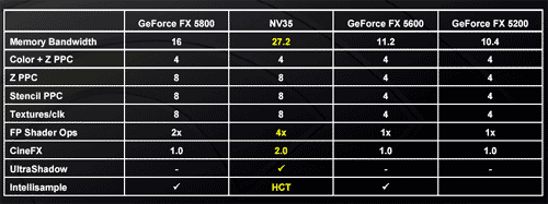
As you can see, there is sufficient hardware in the NV35 to guarantee a throughput of 8 pixels per clock in most scenarios, but in older games (e.g. single textured games) the GPU is only capable of delivering 4 pixels per clock. If you correctly pack the instructions that are dispatched to the execution units in this stage you can yield significantly more than 8 pixel shader operations per clock. For example, in NVIDIA's architecture a multiply/add can be done extremely fast and efficiently in these units, which would be one scenario in which you'd yield more than 8 pixel shader ops per clock.
It all depends on what sort of parallelism can be extracted from the instructions and data coming into this stage of the pipeline. Although not as extreme of a case (there isn't as much parallelism in desktop applications), CPUs enjoy the same difficulty of characterization. For example, the AMD Athlon XP has a total of 9 execution units, but on average the processor yields around 1 instruction per clock; the overall yield of the processor can vary so much depending on available memory bandwidth and the type of data it's working on among other things.
ATI's R3xx architecture differs from NVIDIA slightly in this respect, as they are able to output 8 pixels per clock in every one of the situations listed above. The advantage isn't huge as it is mostly limited to older games, but the difference does exist and is worth pointing out.


19 Comments
View All Comments
Anonymous User - Thursday, October 16, 2003 - link
After reading this article, how can I determine which GeForceFX 5600 card has the NV30 core or the NV35 core. I'm currently interested in purchasing one, but on any of the retail boxes or manuals from the manufacturer's web site say nothing about the type of core used. Did NVidia corrected themselves using the NV35 core before releasing their 5600 cards to the market? Or are there 5600's NV30 cards on the retail shelves too. Help is appreciated. Thanks.JamesVon - Thursday, December 27, 2018 - link
Have you tried to play any Fortnite in GeForceFX 5600? Actually you can get free v-bucks or free fortnite leaked skins here if you interested <a href="https://newfortnite.com/">https://newfortn...Anonymous User - Saturday, September 6, 2003 - link
You should be ashamed. The linking of words to completely unrelated MARKETING ADS is absolutely ridiculous...as if you don’t have ENOUGH ads already.-J
Shagga - Saturday, August 9, 2003 - link
I certainly found the article informative. I read the article with a view to making a decision on which card to purchase over the next week or so and to be honest the article said enough to convince me to sit tight. I also felt there is more to come from both ATI and nVidia and the results which are presented are perhaps not entirely complete. This is pointed out by Anand and at $499 I need to be making the right choice, however, Anand did succeed in convincing me to wait a tad longer.Good article I thought.
Anonymous User - Friday, August 1, 2003 - link
Please stop using Flash graphics!JamesVon - Thursday, December 27, 2018 - link
What is the problem with Flash Graphics? Have you tried using Steam Platform? You can get free steam keys here https://steamity.com if you want to download free steam gamesPete - Tuesday, July 22, 2003 - link
It's only fair that I praise the article, as well. As I said above, in the initial article comment thread, I congratulated Anand on what I thought was a well-written article. I appreciate his lengthy graphics pipeline summary, his extensive image quality investigation, and his usual even-handed commentary (though I had problems with the latter two).Pete - Tuesday, July 22, 2003 - link
I think this is a great article with a few significant flaws in its benchmarking.Firstly, the Doom 3 numbers. Anand acknowledged that he could not get the 9800P 256MB to run the tech demo properly, yet he includes the numbers anyway. This strikes me as not only incorrect but irresponsible. People will see 9800P 256MB numbers and note that its extra memory makes no difference over its 128MB sibling, yet only if they read the article carefully would they know that the driver Anand used limits the 9800P 256MB to only 128MB, essentially crippling the card.
Also, note the difference between Medium Quality and High Quality modes in Doom 3 is only anisotropic filtering (AF), which is enabled in HQ mode. Note that forcing AF in the video card's drivers, rather than via the application, will result in higher performance and potentially lower image quality! This was shown to be the case both in a TechReport article on 3DM03 ("3DMurk"), in forum discussions at B3D, and in an editorial at THG. Hopefully this will be explored fully once a Doom3 demo is released to the public, and we have more open benchmarking of this anticipated game.
Secondly, Anand's initial Quake 3 5900U numbers seemed way off compared to other sites that tested the same card in similar systems at the same settings. At 1600x1200 with 4xAA 8xAF, Anand was scoring over 200fps, well higher than any other review. And yet, after weeks of protest in the forum thread on this article, all that happened was the benchmark results for 12x10 and 16x12 were removed. The text, which notes:
"The GeForceFX 5900 Ultra does extremely well in Quake III Arena, to the point where it is CPU/platform bound at 1600x1200 with 4X AA/8X Anisotropic filtering enabled."
was left unchanged, even though it was based on what many assumed were erroneous benchmark data. I can only conclude that the data were indeed erroneous, as they have been removed from the article. Sadly, the accompanying text has not been edited to reflect that.
Thirdly, the article initially tested Splinter Cell with AA, though the game does not perform correctly with it. The problem was that NVIDIA's drivers automatically disable AA if it's selected, yielding non-AA scores for what an unsupsecting reviewer believes is an AA mode. ATi's driver allow AA, warts and all, and thus produce appropriately dimished benchmark numbers, along with corresponding AA errors. The first step at correcting this mistake was to remove all Splinter Cell graphs and place a blurb in the driver section of the review blaming ATi for not disabling AA. Apparently a second step has been taking, expunging Splinter Cell from the article text altogether. Strangely, Splinter Cell is still listed in the article's drop-down menu as p. 25; clicking will bring you to the one last Quake 3 graph with the incorrect analysis, noted above.
Finally, a note on the conclusion:
"What stood out the most about NVIDIA was how some of their best people could look us in the eye and say "we made a mistake" (in reference to NV30)."
What stands out most to me is that NVIDIA still can't look people in the eye and say they made a mistake by cheating in 3DMark03. Recent articles have shown NVIDIA to be making questionable optimizations (that may be considered cheats in the context of a benchmark) in many games and benchmarks, yet I see only a handful of sites attempt to investigate these issues. ExtremeTech and B3D noted the 3DMark03 "optimizations." Digit-Life has noted CodeCreatures and UT2K3 benchmark "optimizations," and Beyond3D and AMDMB have presented pictorial evidence of what appears to be the reason for the benchmark gains. NVIDIA appears to currently foster a culture of cutting corners without the customer's (and, hopefully, reviewer's) knowledge, and they appear reticent to admit it at all.
I realize this post comes off as harsh against both Anand and NVIDIA. In the initial comment thread on this article, I was gentler in my (IMO, constructive) criticism. As the thread wore on for weeks without a single change in the multiple errors perceived in the original article, I gradually became more curt in my requests for corrections. Anand elicits possibly the greatest benefit of the doubt of any online hardware reviewer I know, as I've read his site and enjoyed the mature and thoughtful personality he imbued it with for years. I'm sorry to say his response--rather, his lack of response, as it was only Evan and Kristopher, not Anand, that replied to the original article thread--was wholly unsatisfactory, and the much belated editing of the article into what you read today was unsatisfactory as well. I would have much preferred Anand(tech) left the original article intact and appended a cautionary note or corrected benchmarks and commentary, rather than simply cutting out some of the questionable figures and text.
Consider this post a summation of the criticism posted in the original article thread. I thought they would be useful to put this article in context, and I hope they are taken as constructive, not destructive, criticism. The 5900 is no doubt a superior card to its predecessor. I also believe this article, in its current form, presents an incomplete picture of both the 5900U and its direct competition, ATi's 9800P 256MB. Hopefully the long chain of revelations and commentary sparked by and after this article will result not in hard feelings, but more educated, thorough, and informative reviews.
I look forward to Anandtech's next review, which I believe has been too long in coming. :)
ritaeora - Tuesday, December 11, 2018 - link
I like your review about the GeForce.http://www.linkedin.com/company/free-instagram-fol...
kyrac - Monday, December 24, 2018 - link
I am a user of Nvidia and i have a great experience using it.https://www.linkedin.com/company/virtual-assistant...