The Apple iPhone 6s and iPhone 6s Plus Review
by Ryan Smith & Joshua Ho on November 2, 2015 8:00 AM EST- Posted in
- Smartphones
- Apple
- Mobile
- SoCs
- iPhone 6s
- iPhone 6s Plus
Analyzing Apple A9’s SoC
For Apple’s engineering teams, I’m still undecided whether Apple’s tick-tock style of SoC development is a curse or a blessing. That Apple more strongly invests in SoC development for the iPhone-S processors is a blessing, as it gives the engineering teams a bit of time to breathe and to plan out major architecture shifts over two years. On the other hand even for non-S iPhones the engineering teams still need to deliver an amazing product – iPhone 5 and iPhone 6 were no slouches – so I’m not sure how much of a breather the engineering teams actually get. They may have two years to space some of their transitions, but they must continue to deliver a top-tier SoC every year.
When Apple released the A7 SoC alongside the iPhone 5s in 2013, they pulled off something that rocked the SoC industry. The Cyclone CPU core all but came out of nowhere, beating previous estimates for the first ARMv8 64-bit phone SoCs (by any vendor) by roughly a year. As a result the 64-bit transition became a lot more important a lot sooner than anyone was expecting, and to this date some of Apple’s SoC competitors are still trying to recover from the shock of having to scramble to go 64-bit sooner than they planned.
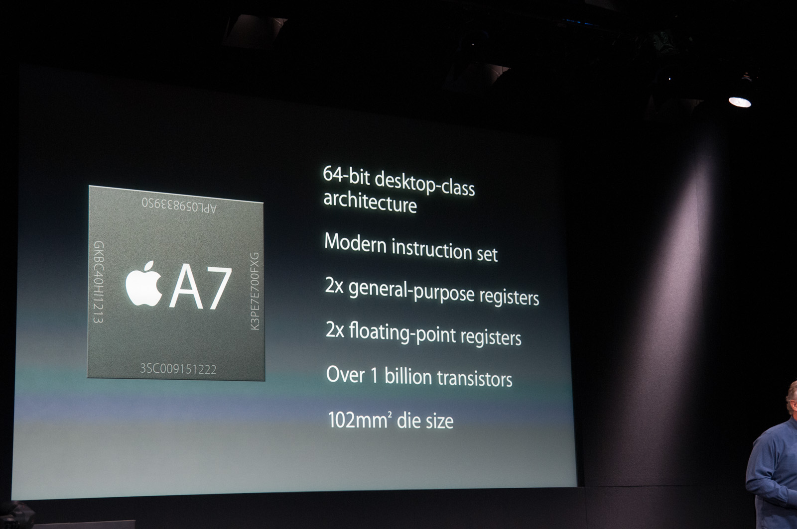
As for Apple’s engineering teams, that we’re on another iPhone-S year means that there’s quite a bit of pressure to pull off a repeat performance, and I suspect that pressure is internal as much as it is external. A7 brought with it Cyclone, a CPU that was not only 64-bit, but thanks to its exceptional (for a mobile CPU) issue width of 6 micro-ops, brought with it a huge jump in single-threaded performance. At the same time A7 also saw Apple transition to PowerVR’s Rogue architecture GPUs (PowerVR G6xxx), which was a similar jump in GPU capabilities and performance, along with setting the stage for Apple’s proprietary, low-level Metal graphics API. A7 was everything Apple needed and more, cementing Apple’s place as a top-tier SoC designer and laying the groundwork for the performance advantage Apple has enjoyed over the past two years.
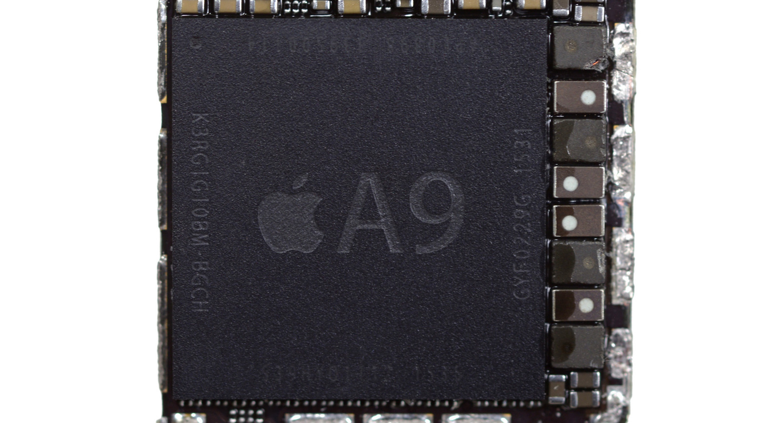
Apple's A9 SoC (Image Courtesy iFixit)
For 2015 then and for their latest iPhone-S, Apple has once again turned out a new SoC. This brings us to the A9, and in a year with an iPhone-S and almost no external design changes to speak of, all eyes are on what Apple has devised to go inside their phones.
| Apple A9 vs A8 SoCs | ||||
| Apple A9 (2015) | Apple A8 (2014) | |||
| Manufacturing Process | TSMC 16nm FinFET / Samsung 14nm FinFET |
TSMC 20nm HKMG | ||
| Die Size | 104.5mm2/96mm2 | 89mm2 | ||
| CPU | 2 x Apple Twister ARMv8 64-bit cores |
2 x Apple Typhoon ARMv8 64-bit cores |
||
| GPU | IMG PowerVR GT7600 | IMG PowerVR GX6450 | ||
Finally Fabbed with FinFETs
When the iPhone 6 launched I spent some time talking about how for the A8 SoC, Apple finally reached the point where they were building SoCs on a leading edge manufacturing process. That process at the time being TSMC’s 20nm planar process. The fact that Apple was building on a leading edge process was important for two reasons: 1) It was a strong indicator of how serious they were about SoC production and how much they were willing to spend in order to achieve the best possible performance, and 2) it meant that Apple had finally completely climbed the ladder (so to speak) and wouldn’t be able to “exceed the curve” just by catching up on manufacturing technology. Post-A8, Apple can only improve their performance by improving their architecture, building bigger chips, and finally, jumping to newer manufacturing processes as they become available.
What wasn’t said at the time – due to the fact that no one outside the fabs was quite sure – was where Apple would go in 2015. Had you asked me in 2014 what I would expect the A9 to be fabbed on, I would have suggested another round on TSMC’s 20nm process now that Apple had caught up to the leading edge. However much to my surprise (and to a steak dinner I lost a bet on) Samsung was able to get their 14nm FinFET process yielding well enough to supply Exynos 7420 in bulk for the Galaxy S6 launch nearly 6 months ago.
The fact that one of the contract fabs was able to get a FinFET process up and yielding well enough for volume production before the very end of 2015 has definitely changed the picture for what Apple can do. Once again they get to jump to a new manufacturing process for their next SoC, though this time by staying on the leading edge.
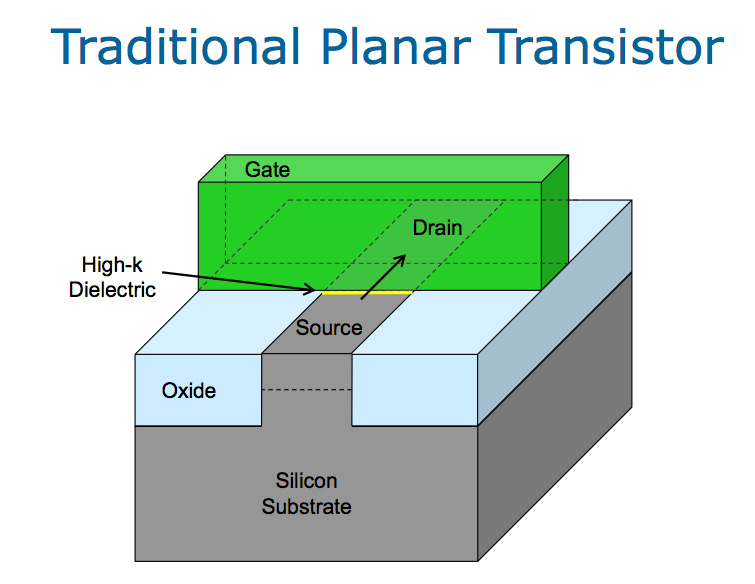
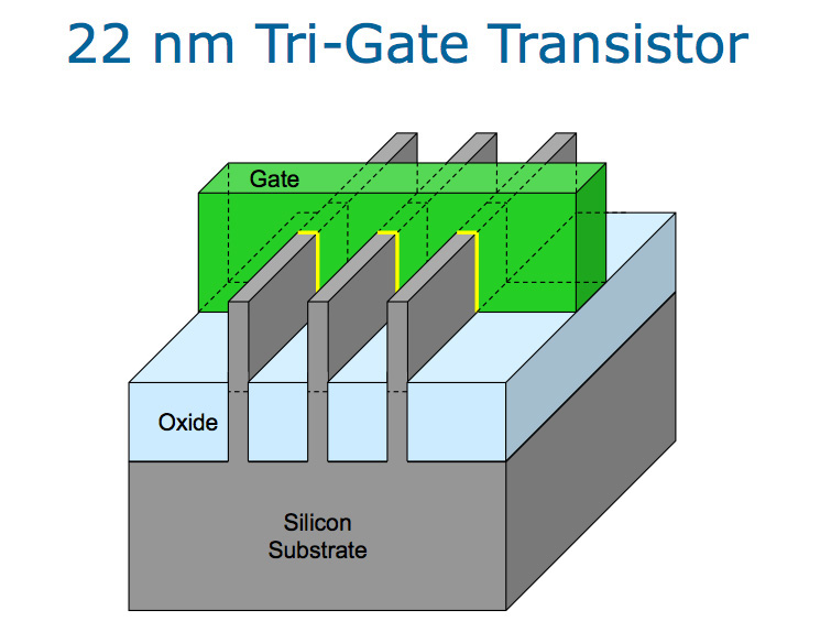
Planar vs. FinFET (3D) Transistors (via Intel)
While I’m not going to go into the physics of FinFET in depth here – we have some great articles on that already – I do want to quickly touch upon why this is so important. 14nm (and 16nm) FinFET isn’t just a new manufacturing node, but it’s part of a broader change in how transistors are manufactured. Simply put, FinFET (aka 3D transistors) are a long in development technology meant to help transistors scale to increasingly small scales, on the order of dozens of atoms or less.
FinFET transistors are necessary because as transistors get smaller their leakage (wasted power) goes up, and without FinFETs leakage would spiral out of control. In fact that’s exactly what happened on the 20nm nodes from Samsung and TSMC; both companies thought the leakage of planar transistors could be adequately controlled at 20nm, only for leakage to be a bigger problem than they expected. Due in large part to this reason, the 20nm SoCs released over the last 18 months have more often than not struggled with power consumption and heat, especially at higher clockspeeds. Apple is something of the exception here, with the 20nm A8 proving to be a solid SoC, thanks in part to their wide CPU design allowing them to achieve good performance without using high clockspeeds that would exacerbate the problem.
That said, while Apple managed to handle 20nm well enough, they were still ultimately at the mercy of a subpar process. The 14nm/16nm FinFET processes are what 20nm should have been all along, with the use of FinFETs drastically cutting down on leakage and reducing operating voltages – and now that FinFETs are here Apple no longer has to be as conservative as they were with A8. What that gives Apple then is a chance to push the envelope much harder on clockspeeds, taking their already wide CPU designs and turning up the clockspeeds as well.


531 Comments
View All Comments
blackcrayon - Monday, November 2, 2015 - link
I bet it goes further than you think. I bet Anandtech is paying Huawei and Samsung or maybe has undercover agents at Qualcomm to make sure their SOCs perform more slowly than Apple's. It's the only way to explain it!You're so enraged and deluded that you can't see how something that is pretty much universally agreed as "one of the best" could possible be "the best" in someone's opinion (an opinion backed up by a uniquely large amount of test data I should add).
osxandwindows - Monday, November 2, 2015 - link
You and your conspiracy theories.lol
So what other conspiracy theories do you have about anandtech
blackcrayon - Wednesday, November 4, 2015 - link
Maybe Apple injected code into Webkit (that's also in Chrome and that Microsoft and Mozilla also copied unbeknownst to them) that makes any bar graph showing iPhone performance to have longer lines! Except when smaller lines are better, then it makes them shorter. :)melgross - Monday, November 2, 2015 - link
Maybe because it actually is the best, despite what Android users want to think.zeeBomb - Monday, November 2, 2015 - link
the fight between android and apple will never end.itpromike - Monday, November 2, 2015 - link
Paid? That is a very dangerous and very serious accusation for a publication such as Anandtech which does scientific and objective chip architectural analysis as well as benchmarks and performance measurements. You are suggesting that Apple is literally giving them money to lie to all of their readers and to willingly change benchmark results AND architectural analysis, including forging SOC cross section pictures (also implicating chip works of being equally fraudulent and deceitful)? You are truly saying that Apple is paying Anandtech to publish falsified results, with Anandtech having no integrity at all? WOW. That is a BOLD BOLD claim. I'd love to see your journalistic proof of this. Do you have links to bank statements, written contracts, emails, phone conversation recordings, etc... that we all can look at so we can make sure the public is aware that Anandtech writers, and analysts are liars? Or can you share with us your deep examination and analysis of the page by page writings and findings in the review in contrast to your on findings that you've spent hours on end testing and analyzing? This way none of their readers will mistake them for being an honest, data driven publication. Just go ahead and link to your findings in the reply to this message. ThanksAlexey291 - Tuesday, November 3, 2015 - link
Er are you sure you're not confusing anandtech from half a dozen years ago with a marketing publication with the same name in the now?shadowii - Monday, November 2, 2015 - link
Wow, what a worthless reply. Read the article.KoolAidMan1 - Monday, November 2, 2015 - link
Anandtech backed up their conclusion with pages and pages of objective tests and analysis. This bothers you so you accuse them of being paid shills.Standard Fandroid in the wild, ladies and gentlemen.
Ethos Evoss - Monday, November 2, 2015 - link
Yeah and final words section like wtitting a bokk !!! Fkin never seen end so long like this..The whole review - aplle bible.. anandtech had to follow apples bible......