The Intel Skylake Mobile and Desktop Launch, with Architecture Analysis
by Ian Cutress on September 1, 2015 11:05 PM ESTA small portion of this page was posted as part of our initial Skylake-K coverage.
The High Level Core
Taking a high level view, the application of the Skylake-S/H architecture features results in the following:
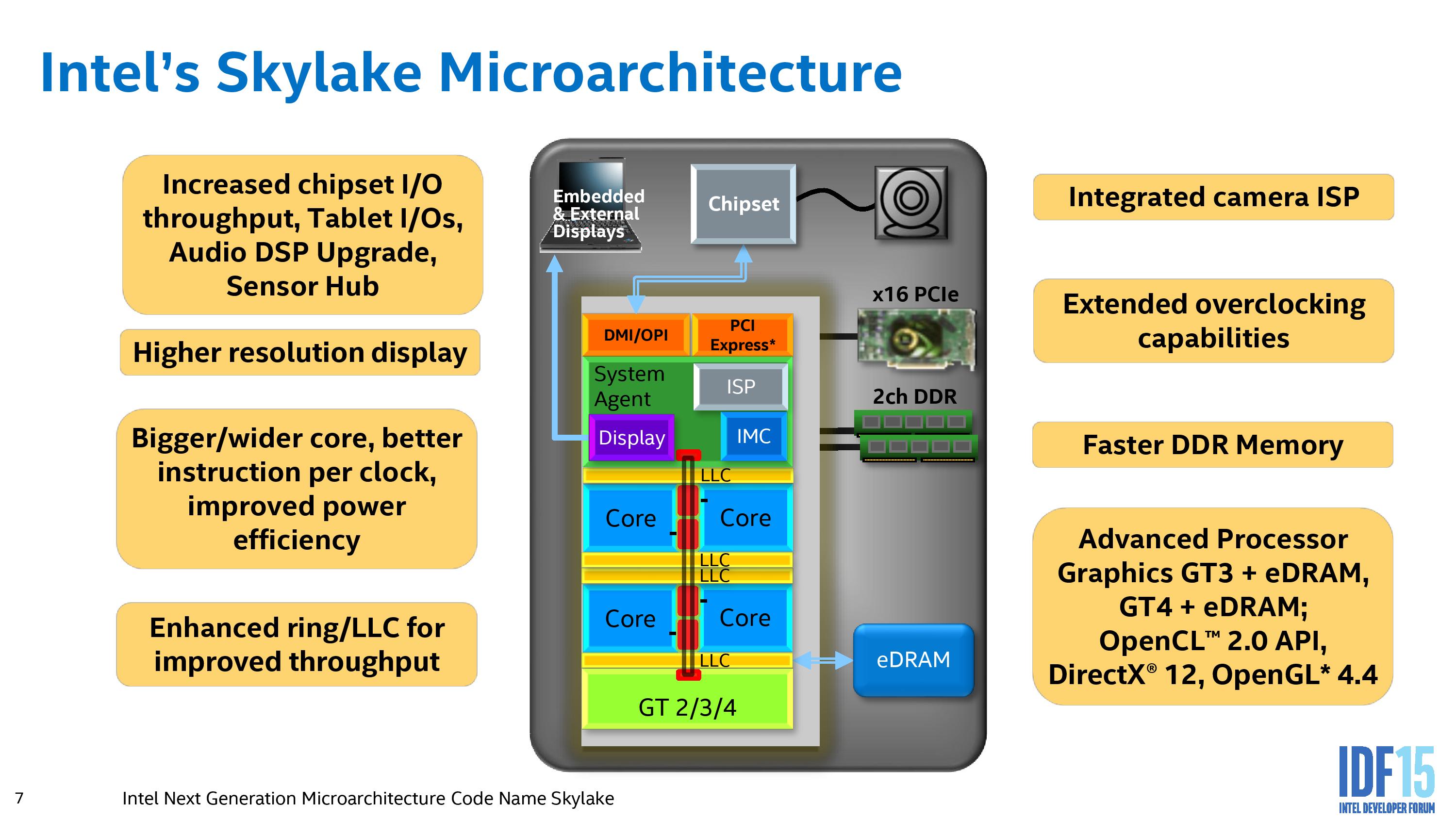
From most perspectives, the central image provided by Intel could have been taken from a Broadwell presentation if you scrubbed out the ‘GT4’ element of the design, but the move to Skylake suggests improvements in each of these areas either in terms of functionality, bandwidth, power consumption, or all of the above.
Out of the box, the Skylake IA core is designed to extract instruction level parallelism from code, and the design allows for more operations to be dispatched, queued and retired in a single clock. We cover this more in the next page. But to augment this, the data transfer ring between cores, cache, graphics and the system agent is also increased in read bandwidth to 128b, allowing more data to be supplied to the cores. In terms of the cores themselves, the big upgrades surround in-flight management of data, especially with respect to cache misses. We have been told that a number of these upgrades, while they might not be readily usable by current software, should have effects in certain vertical markets (finance, big data, etc).
From a memory connectivity standpoint, most processors will support both DDR3L and DDR4 with a dual memory controller design (or a single memory controller that supports both). Skylake-Y (Core M) is the exception here, and will only work in DDR3L/LPDDR3 modes. As always with multi-DRAM support designs, only one standard can be in use at any time.
On the PCI-Express Graphics allocation side, the Skylake-H and Skylake-K processors will have sixteen PCIe 3.0 lanes to use for directly attached devices to the processor, similar to Intel's previous generation processors. These can be split into a single PCIe 3.0 x16, x8/x8 or x8/x4/x4 with basic motherboard design. (Note that this is different to early reports of Skylake having 20 PCIe 3.0 lanes for GPUs. It does not.)
With this SLI will work up to x8/x8 and CrossFire to x8/x8 or x8/x4/x4 in both desktop and mobile designs. For desktops, if a motherboard supports x8/x4/x4 and a PCIe card is placed into that bottom slot, SLI will not work because only one GPU will have eight lanes. NVIDIA requires a minimum of PCIe x8 in order to enable SLI. Crossfire has no such limitation, which makes the possible configurations interesting. Below we discuss that the chipset has 20 (!) PCIe 3.0 lanes to use in five sets of four lanes, and these could be used for graphics cards as well. That means a motherboard can support x8/x8 from the CPU and PCIe 3.0 x4 from the chipset and end up with either dual-SLI or tri-CFX enabled when all the slots are populated.
For Skylake-U/Y, these processors are not typically paired with discrete graphics and as far as we can tell, the PCIe lanes have been removed from these lines. As a result, any storage based on PCIe (such as M.2) for devices based on these processors will be using the chipset PCIe lanes. As mentioned later, the chipsets on U/Y also differ to their more desktop oriented counterparts.
DMI 3.0
The Skylake-S and H processors are connected to the chipset by the four-lane DMI 3.0 interface. The DMI 3.0 protocol is an upgrade over the previous generation which used DMI 2.0 – this upgrade boosts the speed from 5.0 GT/s (2GB/sec) to 8.0 GT/s (~3.93GB/sec), essentially upgrading DMI from PCIe 2 to PCIe 3, but requires the motherboard traces between the CPU and chipset to be shorter (7 inches rather than 8 inches) in order to maintain signal speed and integrity. This also allows one of the biggest upgrades to the system, chipset connectivity, as shown below in the HSIO section.
Skylake-Y/H, by virtue of having the chipset on the processor package, can keep the interface between the CPU and IO very simple and uses what they call an OPIO – on package input-output. We have seen this as far back as Haswell to deliver 4GB/s of bandwidth at 1pJ/bit, and has been listed as being very power efficient as well as highly scalable.
CPU Power Delivery – Moving the FIVR
Moving on to power arrangements, with Skylake the situation changes as compared to Haswell. Prior to Haswell, voltage regulation was performed by the motherboard and the right voltages were then put into the processor. This was deemed inefficient for power consumption, and for the Haswell/Broadwell processors Intel decided to create a fully integrated voltage regulator (FIVR) in order to reduce motherboard cost and reduce power consumption. This had an unintended side-effect – while it was more efficient (good for mobile platforms), it also acted as a source of heat generation inside the CPU with high frequencies. As a result, overclocking was limited by temperatures and the quality of the FIVR led to a large variation in results. For Broadwell-Y, this also resulted in an increase for the z-height of the processor due to having leveling transistors on the rear of the package. As a result, in order to decrease the z-height of any corresponding product, a hole in the motherboard had to be forged:

For Skylake, the voltage regulation is moved back into the hands of the motherboard manufacturers. This should allow for cooler processors depending on how the silicon works, but it will result in slightly more expensive motherboards.
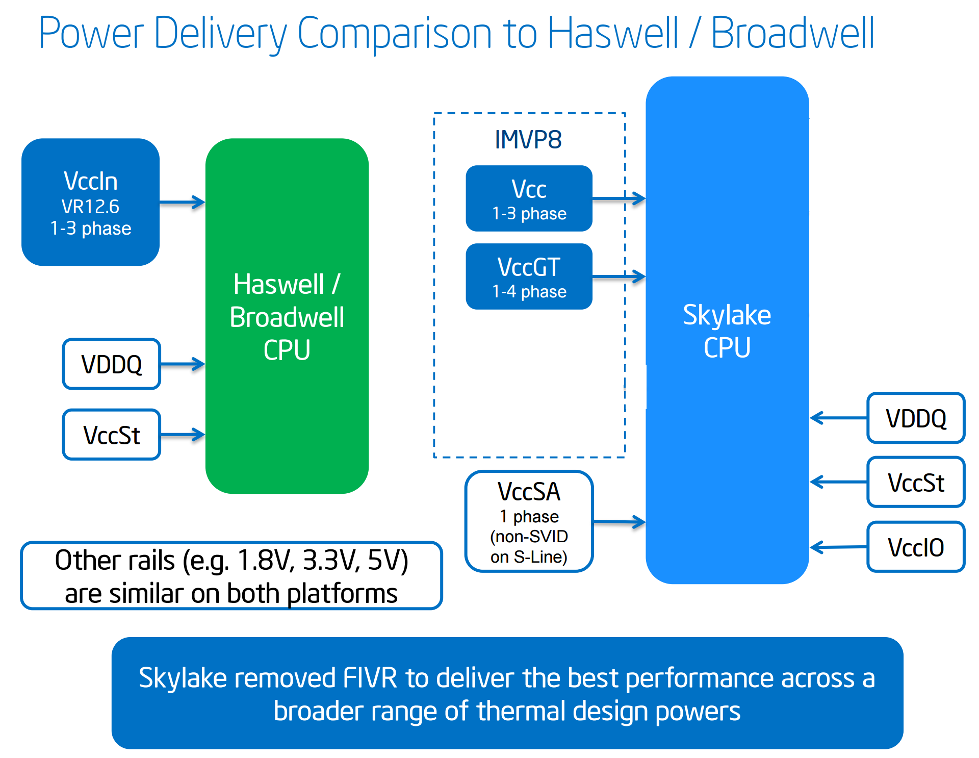
A slight indication of this will be that some motherboards will go back to having a large amount of multiplexed phases on the motherboard, and it will allow some manufacturers to use this as a differentiating point, although the usefulness of such a design is sometimes questionable.


173 Comments
View All Comments
MrSpadge - Wednesday, September 2, 2015 - link
The primary reason Skylake is only qualified for DDR4-2133 is that there is no faster JEDEC standard yet. That's also the reason AT tested at that, I think. However, I agree: restraining an "enthusiast OC CPU" like that seems silly, especially given the very small price premium of significantly faster DDR4. I hope some memory scaling analysis is included in future Skylake articles.techguymaxc - Wednesday, September 2, 2015 - link
Good point, you are correct in that this is the root cause, my analysis suggests the reason is one step further down (or up, depending on your view) the ladder.wintermute000 - Wednesday, September 2, 2015 - link
can the non K chips operate above 2133 or are they locked to 2133 (like non K haswell @ 1600)techguymaxc - Thursday, September 3, 2015 - link
Someone correct me if I'm wrong here, but I believe that is a motherboard feature. As long as you're using a Z series chipset-based motherboard, you *should* be able to run faster memory.MrSpadge - Thursday, September 3, 2015 - link
Sounds plausible.. but noone is talking about that. Damn it! Not even a single review of the regular 6700, and it has been on the shelves in better quantities than the 6700K for 2-3 days (Germany).Impulses - Friday, September 4, 2015 - link
Not available or even listed anywhere yet stateside... :/NikosD - Monday, September 7, 2015 - link
Actually, non K Haswell like Core i7 4790 using a Z chipest can most of the times reach DDR3-2133MHz with no problems.There is only multiplier lock from Intel, not memory lock to 1600MHz.
Xenonite - Thursday, September 3, 2015 - link
Actually, enthusiasts only focus on achieving the lowest possible system power.It seems that most people wouldn't mind further gimping Skylake's performance by underclocking DDR4-2133 to the lowest allowed setting, in the name of needless desktop power savings.
nils_ - Thursday, September 3, 2015 - link
You haven't seen German energy prices ;)Xenonite - Thursday, September 3, 2015 - link
Yea I'm sure there are a lot of readons why we are in this situation (buying a $100 CPU and then having to spend more than that on electricity costs seems a little silly if you are on such a tight budget to begin with); but I still find it increadibly sad that, even if you are willing to spend $1000 on the best CPU performance that money can buy (Xeons aren't overclockable, so a heavily overclocked consumer CPU is normally able to beat almost all single-socket workstations, even in heavily multi-threaded workloads), you are still constrained by some arbitrary power limit.Being willing to spend your hard earned cash on $1000~$2000 of power bills per year still doesn't change the fact that you cannot, and will NEVER be able to, build a system that can make proper use of that amount of power for maximum high-framerate gaming performance.
(Ps. I currently live in South Africa, where our electricity costs are pretty much on par with, and sometimes (if your skin color, like mine, isn't black) even greatly exceeds those of Germany. Heck, once you pass