The Intel Skylake Mobile and Desktop Launch, with Architecture Analysis
by Ian Cutress on September 1, 2015 11:05 PM ESTIntel’s Generation 9 Graphics
On the graphics side of the equation, the information comes in two loaded barrels. For the media capabilities, including information regarding Multi Plane Overlay, Intel’s Quick Sync and HEVC decode, head on over to Ganesh’s great one page summary. Some of that information might be reproduced on this page to help explain some of the more esoteric aspects of the design.
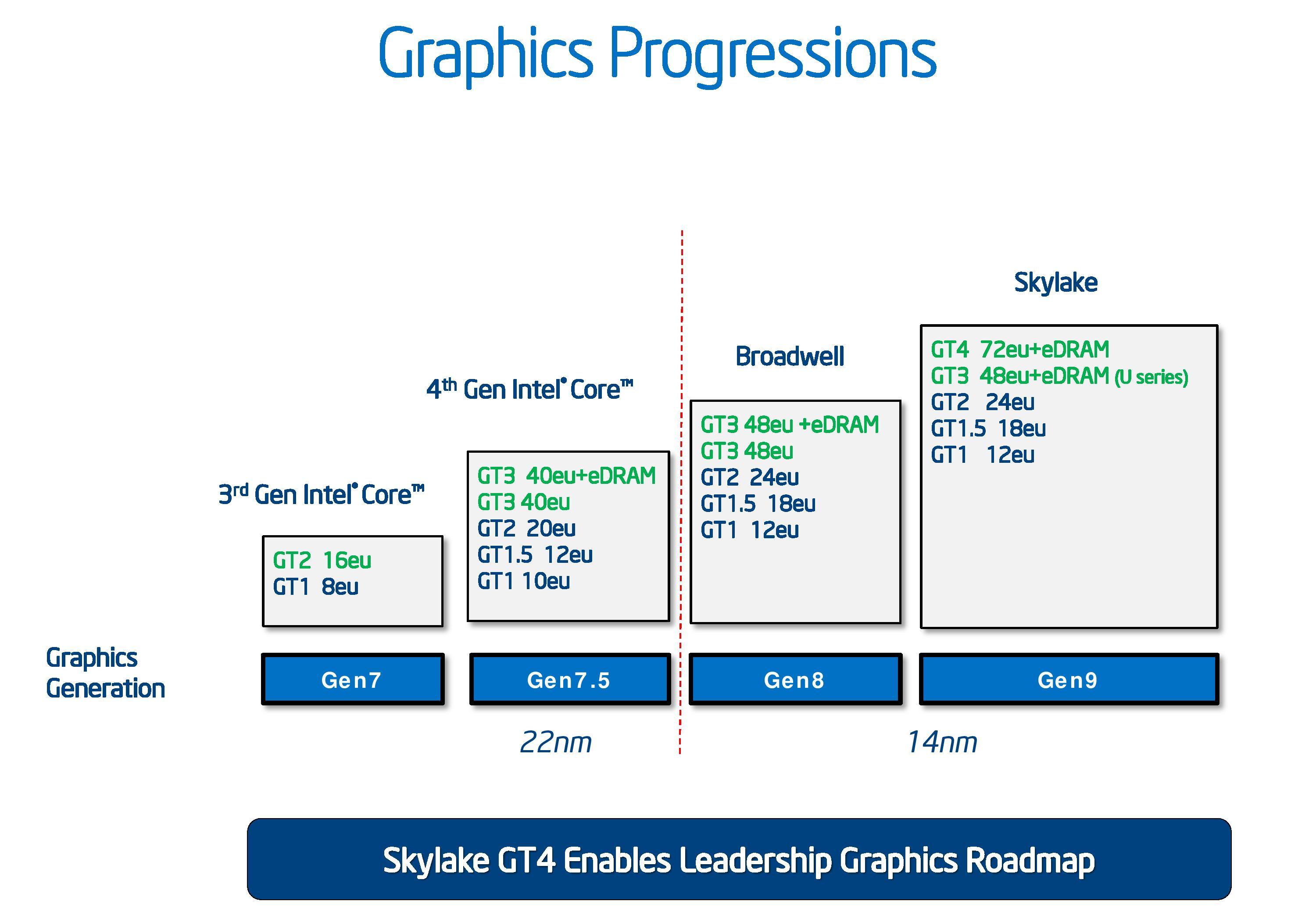
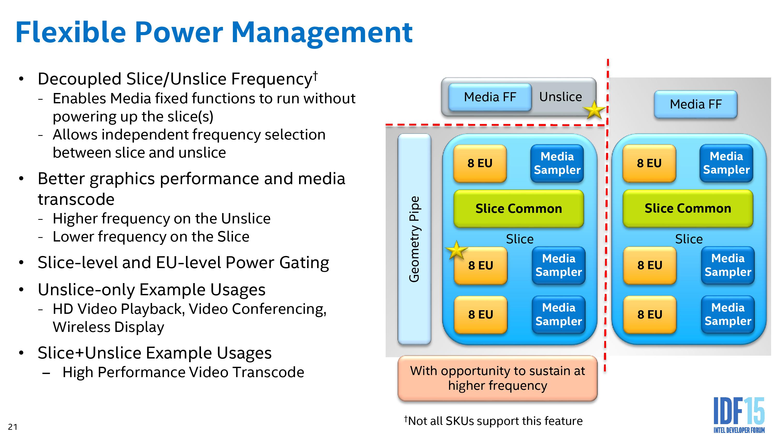
First let us look at how Intel’s integrated graphics has progressed over the generations. It has been no secret that the drive to integrated graphics has eaten almost all of the low end graphics market save one or two cards for extra monitor outputs. For Intel, this means slowly substituting a larger portion of the die to more execution units, as well as upgrading how those units process data. From the graphics above, and as we’ve noted before, Gen9 takes Gen8’s concept but with an added element at the top – GT4, which incorporates a new slice of EUs. As mentioned on the previous page, the eDRAM will come in 64 MB arrangements for GT3e (Iris), and 128 MB for GT4e (Iris Pro).
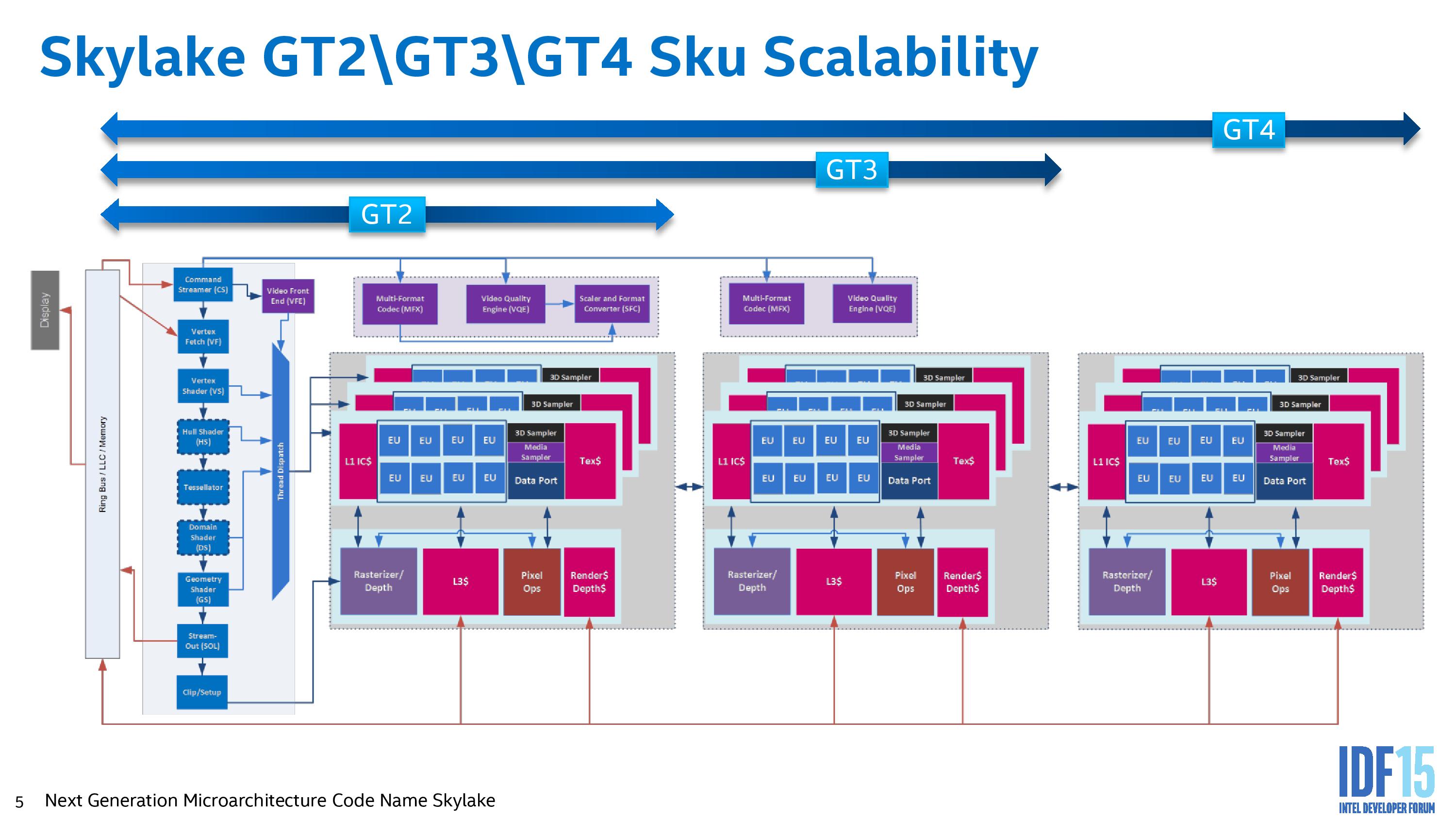
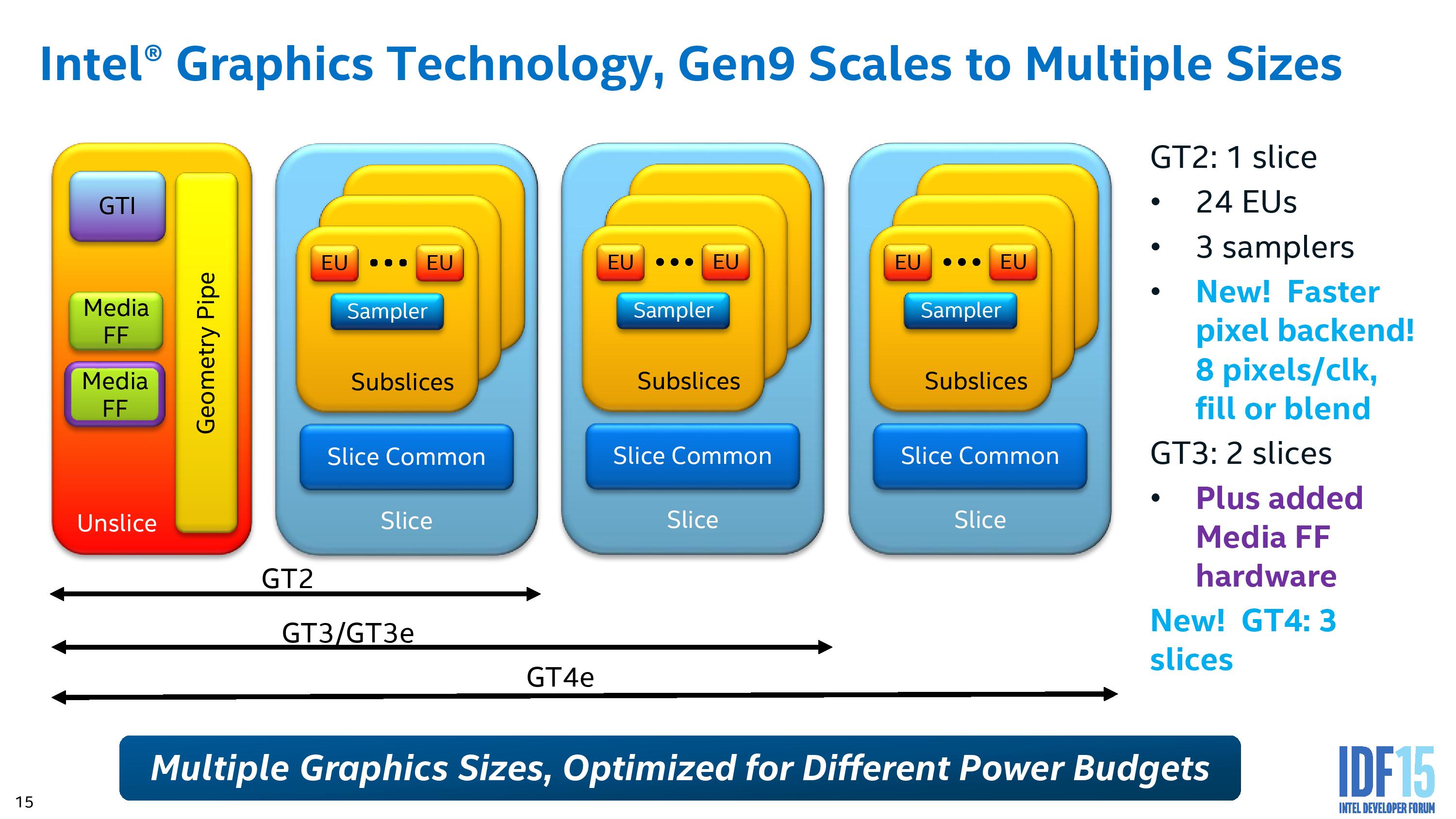
Intel’s graphics topology consists of an ‘unslice’ (or slice common) that deals solely with command streaming, vertex fetching, tessellation, domain shading, geometry shaders, and a thread dispatcher. This is followed up by either one, two or three slices, where each slice holds three sub-slices of 8 EUs, separate L1/L2/L3 caches and rasterizers, texture caches and media samplers. With one slice, a GT2 configuration of 24 EUs, we get the video quality engine (VQE), scalar and format converter (SFC) and a multi format codec engine (MFX). Moving to GT3 adds in another MFX and VQE.
| Intel Gen9 HD Graphics | |||||
| GPU Designation | Execution Units | GT | eDRAM? | YUHS | Example |
| Intel HD Graphics | 12 | 2+1 | - | Y | 4405Y |
| Intel HD Graphics 510 | 12 | 2+2 | - | U S | G4400 4405-U |
| Intel HD Graphics 515 | 24 | 2+2 | - | Y | 6Y75 6Y57 6Y30 |
| Intel HD Graphics 520 | 24 | 4+2 2+2 |
- | U | i7-6600U i3-6100U |
| Intel HD Graphics 530 | 24 | 4+2 2+2 |
- | H S | i7-6700K i3-6100T i7-6820HK |
| Intel HD Graphics P530 | 24 | 4+2 | - | H | E3-1535M v5 |
| Intel Iris Graphics 540 | 48 | 2+3e | 64MB | U | i7-6650U i5-6260U |
| Intel Iris Graphics 550 | 48 | 2+3e | 64MB | U | i7-6567U i3-6167U |
| Intel Iris Pro Graphics 580 | 72 | 4+4e | 128MB | H | - |


In each of the SKU lists, Intel has both the name of the graphics used as well as the base/turbo frequencies of the graphics. To synchronize both the name and the execution unit arrangement, we have the table above. At this point we have no confirmation of any parts having the GT1.5 arrangement, nor are we going to see any 23/24 EU combinations for Pentium/Celeron models similar to what we saw in Haswell. For the 12 EU arrangements, this means that these have a single slice of 24 EUs, but half of them are disabled. We questioned Intel on this back with Haswell, regarding of the EU cuts are split to 4/4/4 from the 8/8/8 sub-slice arrangement, and the answer we got back was interesting – there is no set pattern for 12 EU arrangements. It could be 4/4/4, or 3/4/5, or 3/3/6, or any other combination, as long as the performance is in line with what is expected and the EU count per sub-slice cannot be user probed. Despite the fact that a 3/3/6 arrangement might have L2 cache pressure in some circumstances, Intel feels that at this level of performance they can guarantee that the processors they ship will be consistent. It’s an interesting application.
Part of Intel’s strategy with the graphics is to separate all of these out as much as possible to different frequency planes and power gating, allowing parts of the silicon to only be powered when needed, or to offer more efficiency for regular use cases such as watching video.
The geometry pipe in the un-slice is improved to improve the triangle cull rate as well as remove redundant vertices, which aids an improved tessellated that creates geometry in a format (tri-stips) that can be resubmitted through the triangle cull when needed.

As we noted at Skylake-K launch, Gen 9 graphics also features lossless image compression allowing for fewer data transfers across the graphics subsystem. This saves both power and bandwidth, and an upgrade to the display controller allows the image format to be read in a compressed format so as not to uncompress it before it gets sent out to the display.
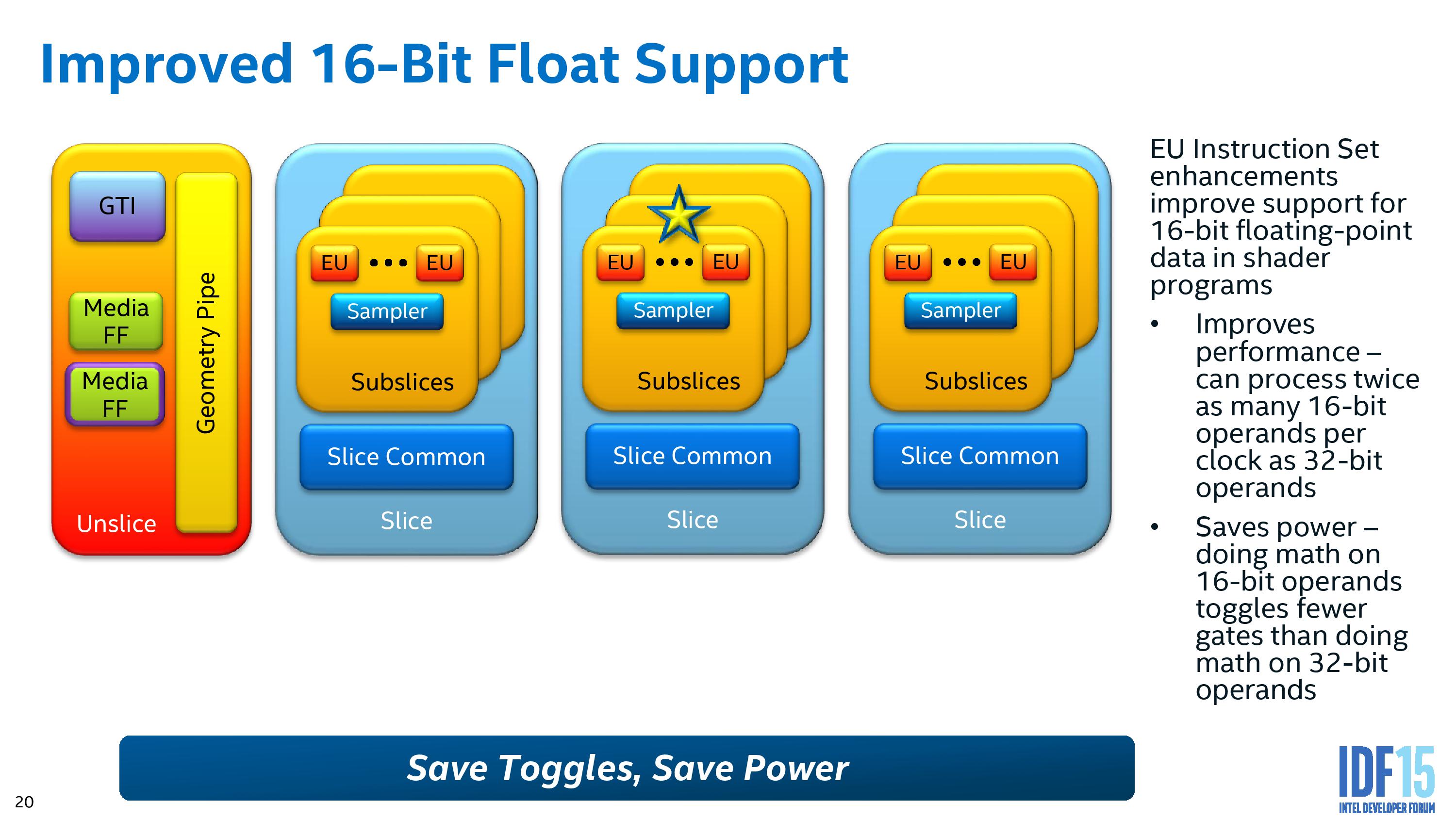
16-bit support has been a key element to discrete graphics in 2014 and 2015, affording faster processing when less accuracy is required by dumping extra significant digits. This is doubly beneficial, resulting in less power consumption for the same amount of work – Intel is exposing this to a greater degree in Gen9 for its shaders.
Intel’s big push on power for low-power Skylake is part of the reason why we did not see much difference in our Skylake-K review. Being able to shut off more parts of the processor that are not in use allows the available power budget to be applied to those that need it, hence why both power gating and frequency domains on the silicon, while they take up die area to implement, contribute to power saving overall or allow work to complete quicker in a race to sleep environment.
Multiplane Overlay (MPO)
One of the features I’m most particularly interested in is Multiplane Overlay. In a typical environment, a user might be looking at content that is stretched, rotated or distorted in some way. In order to perform this transformation, the image information is loaded into memory, siphoned off to the graphics to perform the mathematics, moved back into memory and then fired off to the display controller. This in and out of the DRAM costs power and battery life, so an attempt to mitigate this with fixed function hardware is ultimately beneficial. This is what MPO does.
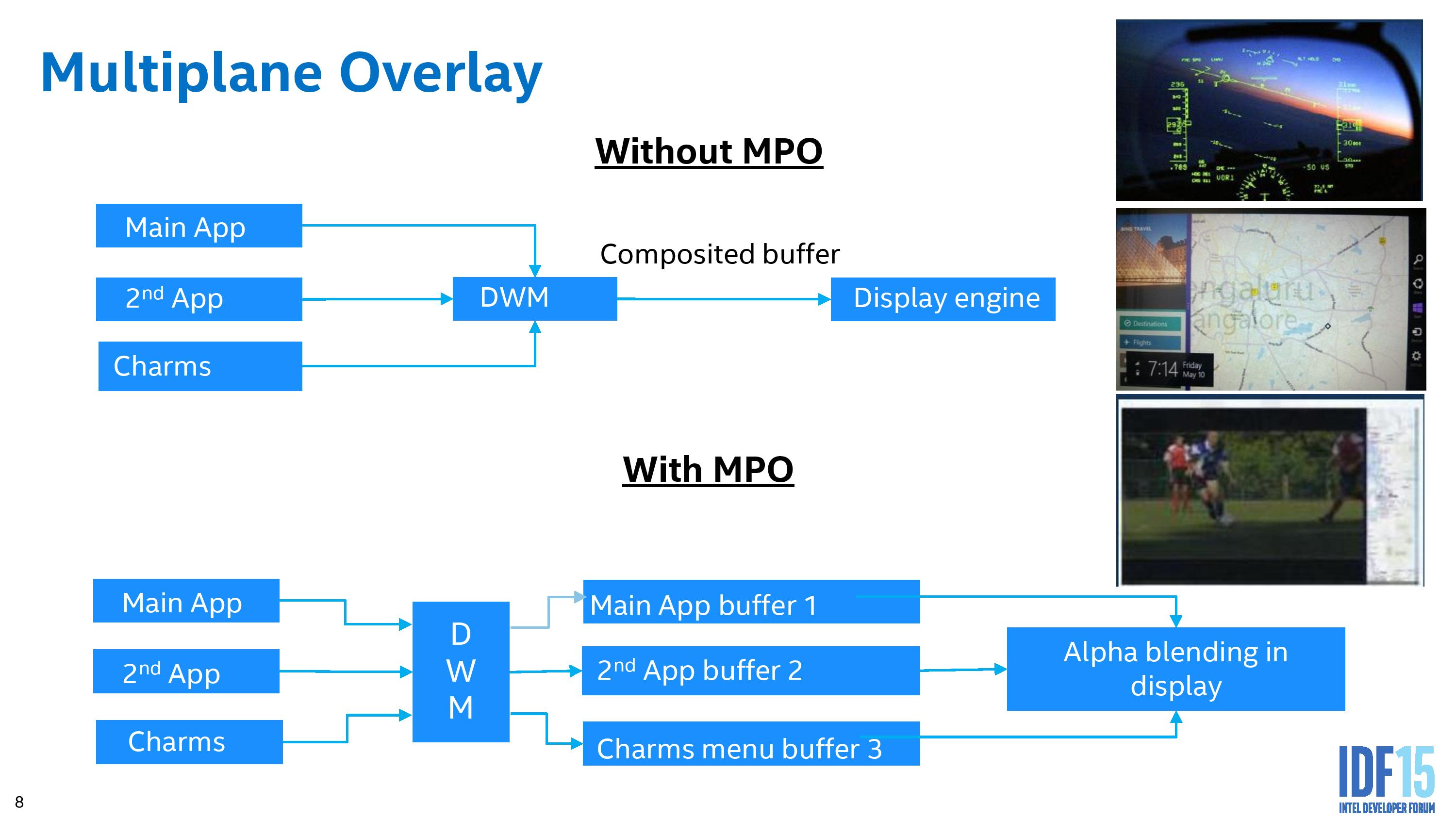
This slides shows a good way on how MPO works. The current implementation splits the screen into three ‘planes’ (app, background, cursor, or any combination therein) which are fired off to the desktop window manager (DWM). In a standard method, these layers are worked on separately before being composited and sent off to the display (the top model). With MPO, each of the planes fills a buffer in fixed function hardware on the display controller, without touching the GPU and requiring it to be put into a high power mode. MPO also allows for data in NV12 format to be processed on the fly as well, rather than requiring it all to be RGB before it is recombined into the final image (which again, saves power and bandwidth).
There are some limitations to this method. Currently, only three planes are supported, and there is no z-hierarchy meaning that if an app is obscured by another but still requires work, and then it does not get discarded as it should. For non-OS work that takes full-screen environments, it also requires the necessary hooks to the FF hardware otherwise it will assume it all as one plane and go back through the GPU. Intel is planning to improve this feature over time, as we might expect.
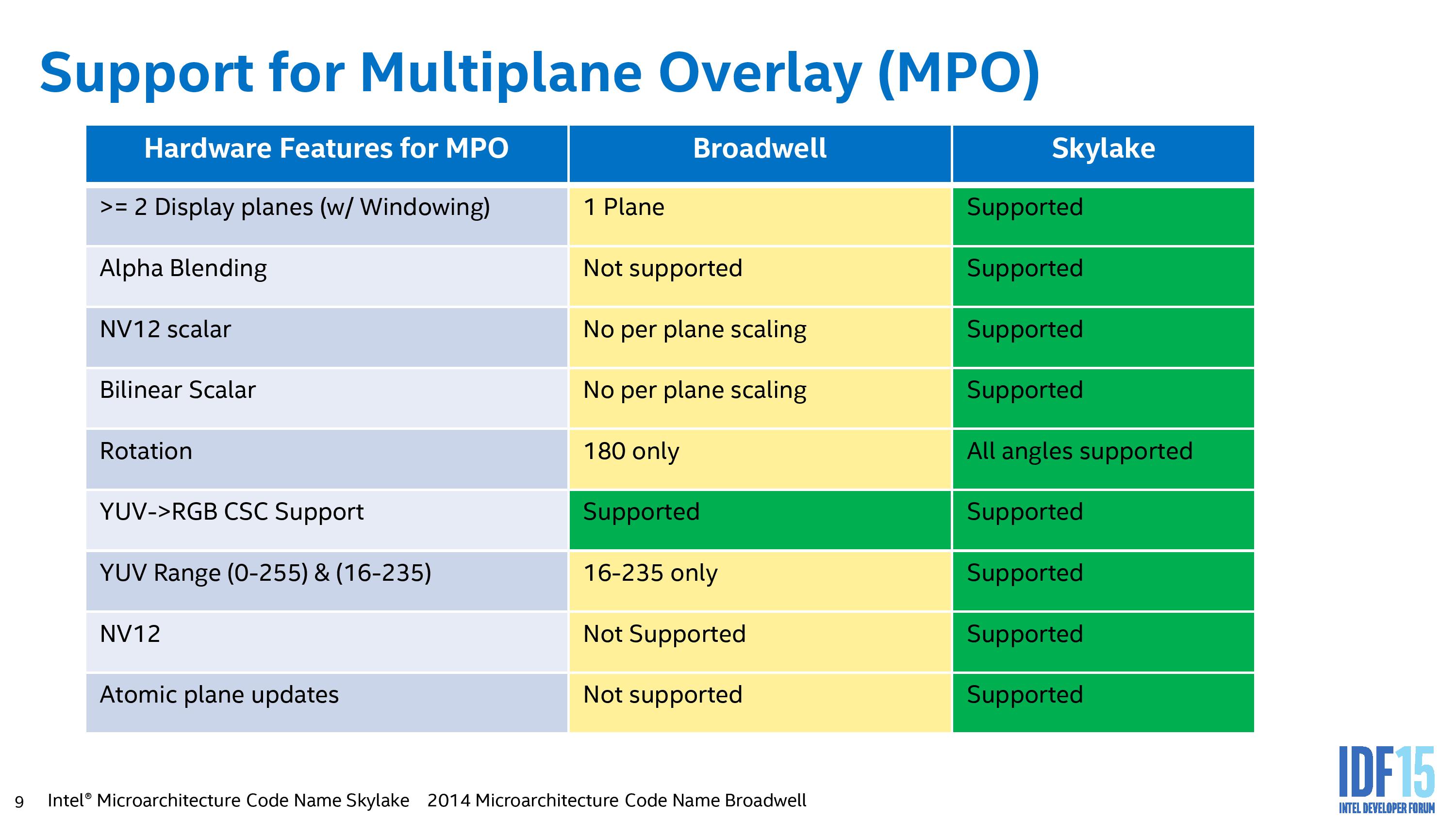
Intel’s data showed a 17% power saving increase overall while watching a 1080p24 video on a 1440p panel. Given the march to higher resolution displays and the lack of high resolution content, I can imagine this being an important player in future content consumption or multitasking.
There are a number of other media specific functions also new to Skylake, especially evolving around RAW processing in the fixed function units of the video quality engines to save power, other memory compression techniques and the encode/decode of specific formats such as HEVC and VP9. For this information, I suggest heading over to read Ganesh’s piece on Intel's Skylake GPU - Analyzing the Media Capabilities.


173 Comments
View All Comments
Xenonite - Thursday, September 3, 2015 - link
Actually, it seems that power consumption is the only thing that matters to consumers, even on the desktop.All this talk about AMD's lack of competition being the reason why we aren't seeing meaningful generational performance improvements is just that: talk.
The real thing that hampers performance progress is consumers' plain refusal to upgrade for performance reasons (even a doubling in performance is not economically viable to produce since no one, except for me it seems, will buy it).
Consumers only buy the lowest power system that they can afford. It has nothing to do with AMD.
Even if AMD released a CPU that is 4x faster than piledriver, it wouldn't change Intel's priority (nor would it help AMD's sales...).
IUU - Wednesday, September 2, 2015 - link
Sorry for my tone , but "I'm failing to see", how transistor count don't mean more to consumers than to anyone else.So, after 10 years of blissful carelessness(because duuude it's user experience dat matters, ugh..),
you will have everyone deceiving you on what they offer on the price point they offer. Very convenient, especially if they are not able to sustain an exponential increase in performance and passing to the next paradigm to achieve it.
Because untill very recently we have been seeing mostly healthy practices, despite the fact that you could always meet people pointing to big or small sins.
Big example, What's the need of an igp on a processor that consumes 90 watts, especially a gpu that is tragically subpar? To hide the fact they have nothing more to offer to the consumer, cpu dependent, at 90 watts(at the current market situation) and have an excuse for charging more on a
theoretically higher consuming and "higher performing" cpu?
Because, what bugs me is what if 6700k lacked the igp? Would it perform better without a useless igp dragging it down? I really don't know, but I feel it wouldn't.
Regarding the mobile solutions and the money and energy limited devices, the igp could really prove to be useful to a lot of people, without overloading their device with a clunky, lowly, discrete gpu.
xenol - Wednesday, September 2, 2015 - link
If the 6700K lacked the iGPU with no other modifications, it would perform exactly the same.MrSpadge - Wednesday, September 2, 2015 - link
Yes, it would perform exaclty the same (if the iGPU is not used, otherwise it needs memory bandwidth). But the chip would run hotter since it would be a lot smaller. Si is not the best thermal conductor, but the presence of the iGPU spreads the other heat producers a bit.xenol - Wednesday, September 2, 2015 - link
I don't think that's how thermals in ICs work...MrSpadge - Wednesday, September 2, 2015 - link
Thermodynamics "work" and don't care if they're being applied to an IC or a metal brick. Silicon is a far better heat conductor than air, so even if the GPU is not used, it will transfer some of the heat from the CPU + Uncore to the heat spreader.My comment was a bit stupid, though, in the way that given how tightly packed the CPU cores and the uncore are, the GPU spreads none of them further apart from each other. It could have been designed like that, but according to the picture on one of first few pages it's not.
Xenonite - Thursday, September 3, 2015 - link
No, it wouldn't. You could easily spread out the cores by padding them with much more cache and doubling their speculative and parallel execution capabilities. If you up the power available for such out of order execution, the additional die space could easily result in 50% more IPC throughput.MrSpadge - Thursday, September 3, 2015 - link
50% IPC increase? Go ahead and save AMD, then! They've been trying that for years with probably billions of R&D budget (accumulated over the years), yet their FX CPUs with huge L3 don't perform significantly better than the APUs with similar CPU cores and no L3 at all.Xenonite - Thursday, September 3, 2015 - link
Yes, but I specifically mentioned using that extra cache to feed the greater amount of speculative execution units made available by the removal of the iGPU.Sadly, AMD can't use this strategy because Global Foundaries' and TSMC's manufacturing technology cannot fit the same amount of transistors into a given area, as Intel's can.
Furthermore, their yields for large dies are also quite a bit lower and AMD really doesn't have the monetary reserves to produce such a high-risk chip.
Also, the largest fraction of that R&D budget went into developing smaller, cheaper and lower power processors to try and enter the mobile market, while almost all of the rest went into sacrificing single threaded design (such as improving and relying more on out of order execution, branch prediction and speculative execution) to design Bulldozer-like, multi-core CPUs (which sacrifice a large portion of die area, that could have been used to make a low amount of very fast cores, to implement a large number of slow cores).
Lastly, I didn't just refer to L3 cache when I suggested using some of the free space left behind by the removal of the iGPU to increase the amount of cache. The L1 and L2 caches could have been made much larger, with more associativity to further reduce the amount and duration of pipeline stalls, due to not having a data dependancy in the cache.
Also, while it is true that the L3 cache did not make much of a difference in the example you posted, its also equally true that cache performance becomes increasingly important as a CPU's data processing throughput increases.
Modern CPU caches just seem to have stagnated (aside from some bandwidth inprovements every now and then), because our CPU cores haven't seen that much of a performance upgrade since the last time the caches have been improved.
Once a CPU gets the required power and transistor budgets for improved out of order performance, the cache will need to be large enough to hold all the different datasets that a single core is working on at the same time (which is not a form a multi-threading in case you were wondering), while also being fast enough to service all of those units at once, without adversely affecting any one set of calculations.
techguymaxc - Wednesday, September 2, 2015 - link
Your representation of Skylake's CPU/IPC performance is inaccurate and incomplete due to the use of the slowest DDR4 memory available. Given the nature of DDR4 (high bandwidth, high latency), it is an absolute necessity to pair the CPU with high clockspeed memory to mitigate the latency impairment. Other sites have tested with faster memory and seen a much larger difference between Haswell and Skylake. See Hardocp's review, (the gaming section specifically) as well as Techspot's review (page 13, memory speed comparison). Hardocp shows Haswell with 1866 RAM is actually faster than Skylake with 2133 RAM in Unigine Heaven and Bioshock Infinite @ lowest quality settings (to create a CPU bottleneck). I find Techspot's article particularly interesting in that they actually tested both platforms with fast RAM. In synthetic testing (Sandra 2015) Haswell with 2400 DDR3 has more memory bandwidth than Skylake with 2666 DDR4, it is not until you pair Skylake with 3000 DDR4 that it achieves more memory bandwidth than Haswell with 2400 DDR3. You can see here directly the impact that latency has, even on bandwidth and not just overall performance. Furthermore in their testing, Haswell with 2400 RAM vs. Skylake with 3000 RAM shows Haswell being faster in Cinebench R15 multi-threaded test (895 vs. 892). Their 7-zip testing has Haswell leading both Skylake configurations in a memory-bound workload (32MB dictionary) in terms of instructions per second. Finally, in a custom Photoshop workload Haswell's performance is once again sandwiched between the two Skylake configurations.Clearly both Haswell and Skylake benefit from faster memory. In fact, Skylake should ideally be paired with > 3000 DDR4 as there are still scenarios in which it is slower than Haswell with 2400 DDR3 due to latency differences.
Enthusiasts are also far more likely to buy faster memory than the literal slowest memory available for the platform, given the minimal price difference. Right now on Newegg one can purchase a 16GB DDR3 2400 kit (2x8) for $90, a mere $10 more than an 1866 16GB kit. With DDR4 the situation is only slightly worse. The cheapest 16GB (2x8) 2133 DDR4 kit is $110, and 3000 goes for $135. It is also important to note that these kits have the same (primary) timings with a CAS latency of 15.
So now we come to your reasoning for pairing Skylake with such slow RAM, and that of other reviewers, as you are not the only one to have done this. Intel only qualified Skylake with DDR4 up to 2133 MT/s. Why did they do this? To save time and money during the qualification stage leading up to Skylake's release. It is not because Skylake will not work with faster RAM, there isn't an unlocked Skylake chip in existence that is incapable of operating with at least 3000 RAM speed, and some significantly higher. Hardocp was able to test their Skylake sample (with no reports of crashing or errors) with the fastest DDR4 currently available today, 3600 MT/s. I have also heard anecdotally from enthusiasts with multiple samples that DDR4 3400-3600 seems to be the sweet spot for memory performance on Skylake.
In conclusion, your testing method is improperly formed, when considered from the perspective of an enthusiast whose desire is to obtain the most performance from Skylake without over-spending. Now, if you believe your target audience is not in fact the PC enthusiast but instead a wider "mainstream" audience, I think the technical content of your articles easily belies this notion.