The Intel Skylake Mobile and Desktop Launch, with Architecture Analysis
by Ian Cutress on September 1, 2015 11:05 PM ESTA small portion of this page was posted as part of our initial Skylake-K coverage.
The High Level Core
Taking a high level view, the application of the Skylake-S/H architecture features results in the following:
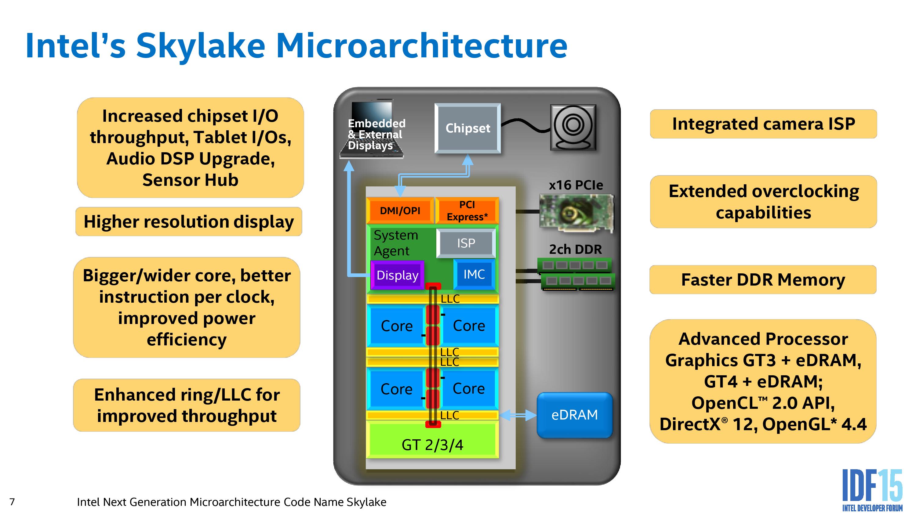
From most perspectives, the central image provided by Intel could have been taken from a Broadwell presentation if you scrubbed out the ‘GT4’ element of the design, but the move to Skylake suggests improvements in each of these areas either in terms of functionality, bandwidth, power consumption, or all of the above.
Out of the box, the Skylake IA core is designed to extract instruction level parallelism from code, and the design allows for more operations to be dispatched, queued and retired in a single clock. We cover this more in the next page. But to augment this, the data transfer ring between cores, cache, graphics and the system agent is also increased in read bandwidth to 128b, allowing more data to be supplied to the cores. In terms of the cores themselves, the big upgrades surround in-flight management of data, especially with respect to cache misses. We have been told that a number of these upgrades, while they might not be readily usable by current software, should have effects in certain vertical markets (finance, big data, etc).
From a memory connectivity standpoint, most processors will support both DDR3L and DDR4 with a dual memory controller design (or a single memory controller that supports both). Skylake-Y (Core M) is the exception here, and will only work in DDR3L/LPDDR3 modes. As always with multi-DRAM support designs, only one standard can be in use at any time.
On the PCI-Express Graphics allocation side, the Skylake-H and Skylake-K processors will have sixteen PCIe 3.0 lanes to use for directly attached devices to the processor, similar to Intel's previous generation processors. These can be split into a single PCIe 3.0 x16, x8/x8 or x8/x4/x4 with basic motherboard design. (Note that this is different to early reports of Skylake having 20 PCIe 3.0 lanes for GPUs. It does not.)
With this SLI will work up to x8/x8 and CrossFire to x8/x8 or x8/x4/x4 in both desktop and mobile designs. For desktops, if a motherboard supports x8/x4/x4 and a PCIe card is placed into that bottom slot, SLI will not work because only one GPU will have eight lanes. NVIDIA requires a minimum of PCIe x8 in order to enable SLI. Crossfire has no such limitation, which makes the possible configurations interesting. Below we discuss that the chipset has 20 (!) PCIe 3.0 lanes to use in five sets of four lanes, and these could be used for graphics cards as well. That means a motherboard can support x8/x8 from the CPU and PCIe 3.0 x4 from the chipset and end up with either dual-SLI or tri-CFX enabled when all the slots are populated.
For Skylake-U/Y, these processors are not typically paired with discrete graphics and as far as we can tell, the PCIe lanes have been removed from these lines. As a result, any storage based on PCIe (such as M.2) for devices based on these processors will be using the chipset PCIe lanes. As mentioned later, the chipsets on U/Y also differ to their more desktop oriented counterparts.
DMI 3.0
The Skylake-S and H processors are connected to the chipset by the four-lane DMI 3.0 interface. The DMI 3.0 protocol is an upgrade over the previous generation which used DMI 2.0 – this upgrade boosts the speed from 5.0 GT/s (2GB/sec) to 8.0 GT/s (~3.93GB/sec), essentially upgrading DMI from PCIe 2 to PCIe 3, but requires the motherboard traces between the CPU and chipset to be shorter (7 inches rather than 8 inches) in order to maintain signal speed and integrity. This also allows one of the biggest upgrades to the system, chipset connectivity, as shown below in the HSIO section.
Skylake-Y/H, by virtue of having the chipset on the processor package, can keep the interface between the CPU and IO very simple and uses what they call an OPIO – on package input-output. We have seen this as far back as Haswell to deliver 4GB/s of bandwidth at 1pJ/bit, and has been listed as being very power efficient as well as highly scalable.
CPU Power Delivery – Moving the FIVR
Moving on to power arrangements, with Skylake the situation changes as compared to Haswell. Prior to Haswell, voltage regulation was performed by the motherboard and the right voltages were then put into the processor. This was deemed inefficient for power consumption, and for the Haswell/Broadwell processors Intel decided to create a fully integrated voltage regulator (FIVR) in order to reduce motherboard cost and reduce power consumption. This had an unintended side-effect – while it was more efficient (good for mobile platforms), it also acted as a source of heat generation inside the CPU with high frequencies. As a result, overclocking was limited by temperatures and the quality of the FIVR led to a large variation in results. For Broadwell-Y, this also resulted in an increase for the z-height of the processor due to having leveling transistors on the rear of the package. As a result, in order to decrease the z-height of any corresponding product, a hole in the motherboard had to be forged:

For Skylake, the voltage regulation is moved back into the hands of the motherboard manufacturers. This should allow for cooler processors depending on how the silicon works, but it will result in slightly more expensive motherboards.
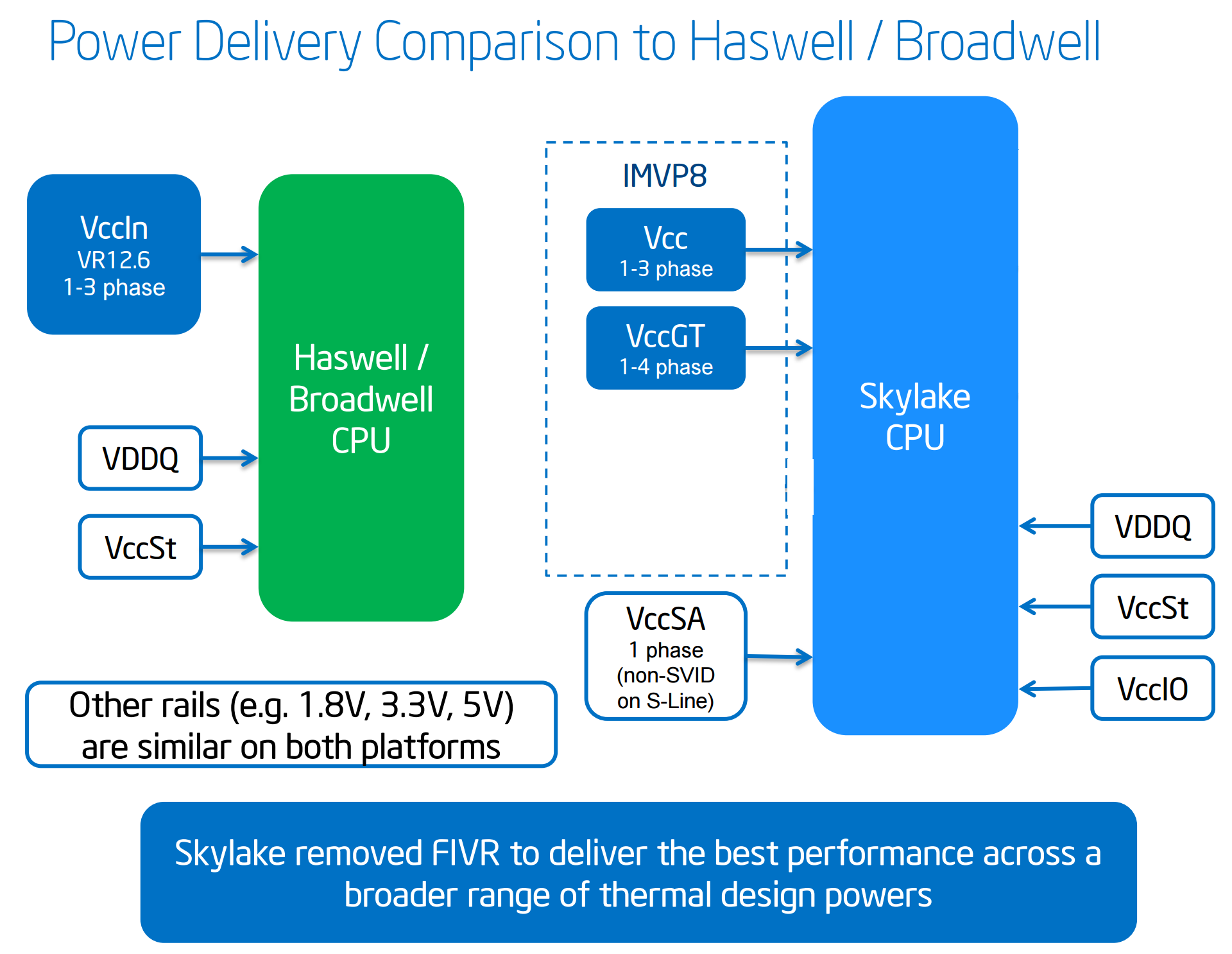
A slight indication of this will be that some motherboards will go back to having a large amount of multiplexed phases on the motherboard, and it will allow some manufacturers to use this as a differentiating point, although the usefulness of such a design is sometimes questionable.


173 Comments
View All Comments
Xenonite - Thursday, September 3, 2015 - link
Actually, it seems that power consumption is the only thing that matters to consumers, even on the desktop.All this talk about AMD's lack of competition being the reason why we aren't seeing meaningful generational performance improvements is just that: talk.
The real thing that hampers performance progress is consumers' plain refusal to upgrade for performance reasons (even a doubling in performance is not economically viable to produce since no one, except for me it seems, will buy it).
Consumers only buy the lowest power system that they can afford. It has nothing to do with AMD.
Even if AMD released a CPU that is 4x faster than piledriver, it wouldn't change Intel's priority (nor would it help AMD's sales...).
IUU - Wednesday, September 2, 2015 - link
Sorry for my tone , but "I'm failing to see", how transistor count don't mean more to consumers than to anyone else.So, after 10 years of blissful carelessness(because duuude it's user experience dat matters, ugh..),
you will have everyone deceiving you on what they offer on the price point they offer. Very convenient, especially if they are not able to sustain an exponential increase in performance and passing to the next paradigm to achieve it.
Because untill very recently we have been seeing mostly healthy practices, despite the fact that you could always meet people pointing to big or small sins.
Big example, What's the need of an igp on a processor that consumes 90 watts, especially a gpu that is tragically subpar? To hide the fact they have nothing more to offer to the consumer, cpu dependent, at 90 watts(at the current market situation) and have an excuse for charging more on a
theoretically higher consuming and "higher performing" cpu?
Because, what bugs me is what if 6700k lacked the igp? Would it perform better without a useless igp dragging it down? I really don't know, but I feel it wouldn't.
Regarding the mobile solutions and the money and energy limited devices, the igp could really prove to be useful to a lot of people, without overloading their device with a clunky, lowly, discrete gpu.
xenol - Wednesday, September 2, 2015 - link
If the 6700K lacked the iGPU with no other modifications, it would perform exactly the same.MrSpadge - Wednesday, September 2, 2015 - link
Yes, it would perform exaclty the same (if the iGPU is not used, otherwise it needs memory bandwidth). But the chip would run hotter since it would be a lot smaller. Si is not the best thermal conductor, but the presence of the iGPU spreads the other heat producers a bit.xenol - Wednesday, September 2, 2015 - link
I don't think that's how thermals in ICs work...MrSpadge - Wednesday, September 2, 2015 - link
Thermodynamics "work" and don't care if they're being applied to an IC or a metal brick. Silicon is a far better heat conductor than air, so even if the GPU is not used, it will transfer some of the heat from the CPU + Uncore to the heat spreader.My comment was a bit stupid, though, in the way that given how tightly packed the CPU cores and the uncore are, the GPU spreads none of them further apart from each other. It could have been designed like that, but according to the picture on one of first few pages it's not.
Xenonite - Thursday, September 3, 2015 - link
No, it wouldn't. You could easily spread out the cores by padding them with much more cache and doubling their speculative and parallel execution capabilities. If you up the power available for such out of order execution, the additional die space could easily result in 50% more IPC throughput.MrSpadge - Thursday, September 3, 2015 - link
50% IPC increase? Go ahead and save AMD, then! They've been trying that for years with probably billions of R&D budget (accumulated over the years), yet their FX CPUs with huge L3 don't perform significantly better than the APUs with similar CPU cores and no L3 at all.Xenonite - Thursday, September 3, 2015 - link
Yes, but I specifically mentioned using that extra cache to feed the greater amount of speculative execution units made available by the removal of the iGPU.Sadly, AMD can't use this strategy because Global Foundaries' and TSMC's manufacturing technology cannot fit the same amount of transistors into a given area, as Intel's can.
Furthermore, their yields for large dies are also quite a bit lower and AMD really doesn't have the monetary reserves to produce such a high-risk chip.
Also, the largest fraction of that R&D budget went into developing smaller, cheaper and lower power processors to try and enter the mobile market, while almost all of the rest went into sacrificing single threaded design (such as improving and relying more on out of order execution, branch prediction and speculative execution) to design Bulldozer-like, multi-core CPUs (which sacrifice a large portion of die area, that could have been used to make a low amount of very fast cores, to implement a large number of slow cores).
Lastly, I didn't just refer to L3 cache when I suggested using some of the free space left behind by the removal of the iGPU to increase the amount of cache. The L1 and L2 caches could have been made much larger, with more associativity to further reduce the amount and duration of pipeline stalls, due to not having a data dependancy in the cache.
Also, while it is true that the L3 cache did not make much of a difference in the example you posted, its also equally true that cache performance becomes increasingly important as a CPU's data processing throughput increases.
Modern CPU caches just seem to have stagnated (aside from some bandwidth inprovements every now and then), because our CPU cores haven't seen that much of a performance upgrade since the last time the caches have been improved.
Once a CPU gets the required power and transistor budgets for improved out of order performance, the cache will need to be large enough to hold all the different datasets that a single core is working on at the same time (which is not a form a multi-threading in case you were wondering), while also being fast enough to service all of those units at once, without adversely affecting any one set of calculations.
techguymaxc - Wednesday, September 2, 2015 - link
Your representation of Skylake's CPU/IPC performance is inaccurate and incomplete due to the use of the slowest DDR4 memory available. Given the nature of DDR4 (high bandwidth, high latency), it is an absolute necessity to pair the CPU with high clockspeed memory to mitigate the latency impairment. Other sites have tested with faster memory and seen a much larger difference between Haswell and Skylake. See Hardocp's review, (the gaming section specifically) as well as Techspot's review (page 13, memory speed comparison). Hardocp shows Haswell with 1866 RAM is actually faster than Skylake with 2133 RAM in Unigine Heaven and Bioshock Infinite @ lowest quality settings (to create a CPU bottleneck). I find Techspot's article particularly interesting in that they actually tested both platforms with fast RAM. In synthetic testing (Sandra 2015) Haswell with 2400 DDR3 has more memory bandwidth than Skylake with 2666 DDR4, it is not until you pair Skylake with 3000 DDR4 that it achieves more memory bandwidth than Haswell with 2400 DDR3. You can see here directly the impact that latency has, even on bandwidth and not just overall performance. Furthermore in their testing, Haswell with 2400 RAM vs. Skylake with 3000 RAM shows Haswell being faster in Cinebench R15 multi-threaded test (895 vs. 892). Their 7-zip testing has Haswell leading both Skylake configurations in a memory-bound workload (32MB dictionary) in terms of instructions per second. Finally, in a custom Photoshop workload Haswell's performance is once again sandwiched between the two Skylake configurations.Clearly both Haswell and Skylake benefit from faster memory. In fact, Skylake should ideally be paired with > 3000 DDR4 as there are still scenarios in which it is slower than Haswell with 2400 DDR3 due to latency differences.
Enthusiasts are also far more likely to buy faster memory than the literal slowest memory available for the platform, given the minimal price difference. Right now on Newegg one can purchase a 16GB DDR3 2400 kit (2x8) for $90, a mere $10 more than an 1866 16GB kit. With DDR4 the situation is only slightly worse. The cheapest 16GB (2x8) 2133 DDR4 kit is $110, and 3000 goes for $135. It is also important to note that these kits have the same (primary) timings with a CAS latency of 15.
So now we come to your reasoning for pairing Skylake with such slow RAM, and that of other reviewers, as you are not the only one to have done this. Intel only qualified Skylake with DDR4 up to 2133 MT/s. Why did they do this? To save time and money during the qualification stage leading up to Skylake's release. It is not because Skylake will not work with faster RAM, there isn't an unlocked Skylake chip in existence that is incapable of operating with at least 3000 RAM speed, and some significantly higher. Hardocp was able to test their Skylake sample (with no reports of crashing or errors) with the fastest DDR4 currently available today, 3600 MT/s. I have also heard anecdotally from enthusiasts with multiple samples that DDR4 3400-3600 seems to be the sweet spot for memory performance on Skylake.
In conclusion, your testing method is improperly formed, when considered from the perspective of an enthusiast whose desire is to obtain the most performance from Skylake without over-spending. Now, if you believe your target audience is not in fact the PC enthusiast but instead a wider "mainstream" audience, I think the technical content of your articles easily belies this notion.