The AMD Radeon R9 Fury Review, Feat. Sapphire & ASUS
by Ryan Smith on July 10, 2015 9:00 AM ESTMeet The ASUS STRIX R9 Fury
Our second card of the day is ASUS’s STRIX R9 Fury, which arrived just in time for the article cutoff. Unlike Sapphire, Asus is releasing just a single card, the STRIX-R9FURY-DC3-4G-GAMING.
| Radeon R9 Fury Launch Cards | |||||
| ASUS STRIX R9 Fury | Sapphire Tri-X R9 Fury | Sapphire Tri-X R9 Fury OC | |||
| Boost Clock | 1000MHz / 1020MHz (OC) |
1000MHz | 1040MHz | ||
| Memory Clock | 1Gbps HBM | 1Gbps HBM | 1Gbps HBM | ||
| VRAM | 4GB | 4GB | 4GB | ||
| Maximum ASIC Power | 216W | 300W | 300W | ||
| Length | 12" | 12" | 12" | ||
| Width | Double Slot | Double Slot | Double Slot | ||
| Cooler Type | Open Air | Open Air | Open Air | ||
| Launch Date | 07/14/15 | 07/14/15 | 07/14/15 | ||
| Price | $579 | $549 | $569 | ||
With only a single card, ASUS has decided to split the difference between reference and OC cards and offer one card with both features. Out of the box the STRIX is a reference clocked card, with a GPU clockspeed of 1000MHz and memory rate of 1Gbps. However Asus also officially supports an OC mode, which when accessed through their GPU Tweak II software bumps up the clockspeed 20MHz to 1020MHz. With OC mode offering sub-2% performance gains there’s not much to say about performance; the gesture is appreciated, but with such a small overclock the performance gains are pretty trivial in the long run. Otherwise at stock the card should see performance similar to Sapphire’s reference clocked R9 Fury card.
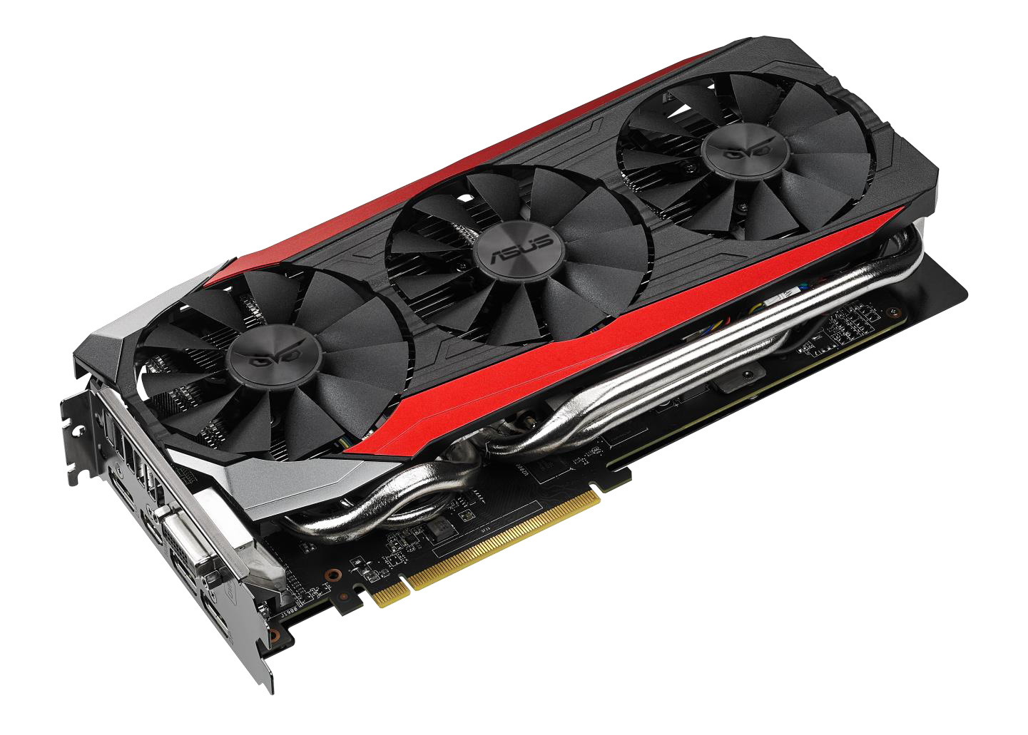
Diving right into matters, for their R9 Fury card ASUS has opted to go with a fully custom design, pairing up a custom PCB with one of the company’s well-known DirectCU III coolers. The PCB itself is quite large, measuring 10.6” long and extending a further .6” above the top of the I/O bracket. Unfortunately we’re not able to get a clear shot of the PCB since we need to maintain the card in working order, but judging from the design ASUS has clearly overbuilt it for greater purposes. There are voltage monitoring points at the front of the card and unpopulated positions that look to be for switches. Consequently I wouldn’t be all that surprised if we saw this PCB used in a higher end card in the future.
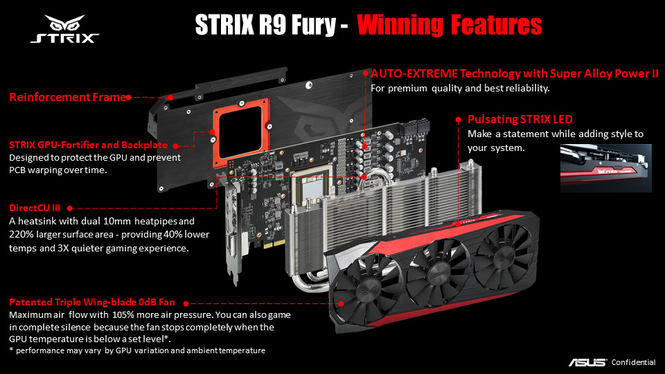
Moving on, since this is a custom PCB ASUS has outfitted the card with their own power delivery system. ASUS is using a 12 phase design here, backed by the company’s Super Alloy Power II discrete components. With their components and their “auto-extreme” build process ASUS is looking to make the argument that the STRIX is a higher quality card, and while we’re not discounting those claims they’re more or less impossible to verify, especially compared to the significant quality of AMD’s own reference design.

Meanwhile it comes as a bit of a surprise that even with such a high phase count, ASUS’s default power limits are set relatively low. We’re told that the card’s default ASIC power limit is just 216W, and our testing largely concurs with this. The overall board TBP is still going to be close to AMD’s 275W value, but this means that Asus has clamped down on the bulk of the card’s TDP headroom by default. The card has enough headroom to sustain 1000MHz in all of our games – which is what really matters – while FurMark runs at a significantly lower frequency than any R9 Fury series cards built on AMD’s PCB as a result of the lower power limit. As a result ASUS also bumps up the power limit by 10% when in OC mode to make sure there’s enough headroom for the higher clockspeeds. Ultimately this doesn’t have a performance impact that we can find, and outside of FurMark it’s unlikely to save any power, but given what Fiji is capable of with respect to both performance and power consumption, this is an interesting design choice on ASUS’s part.

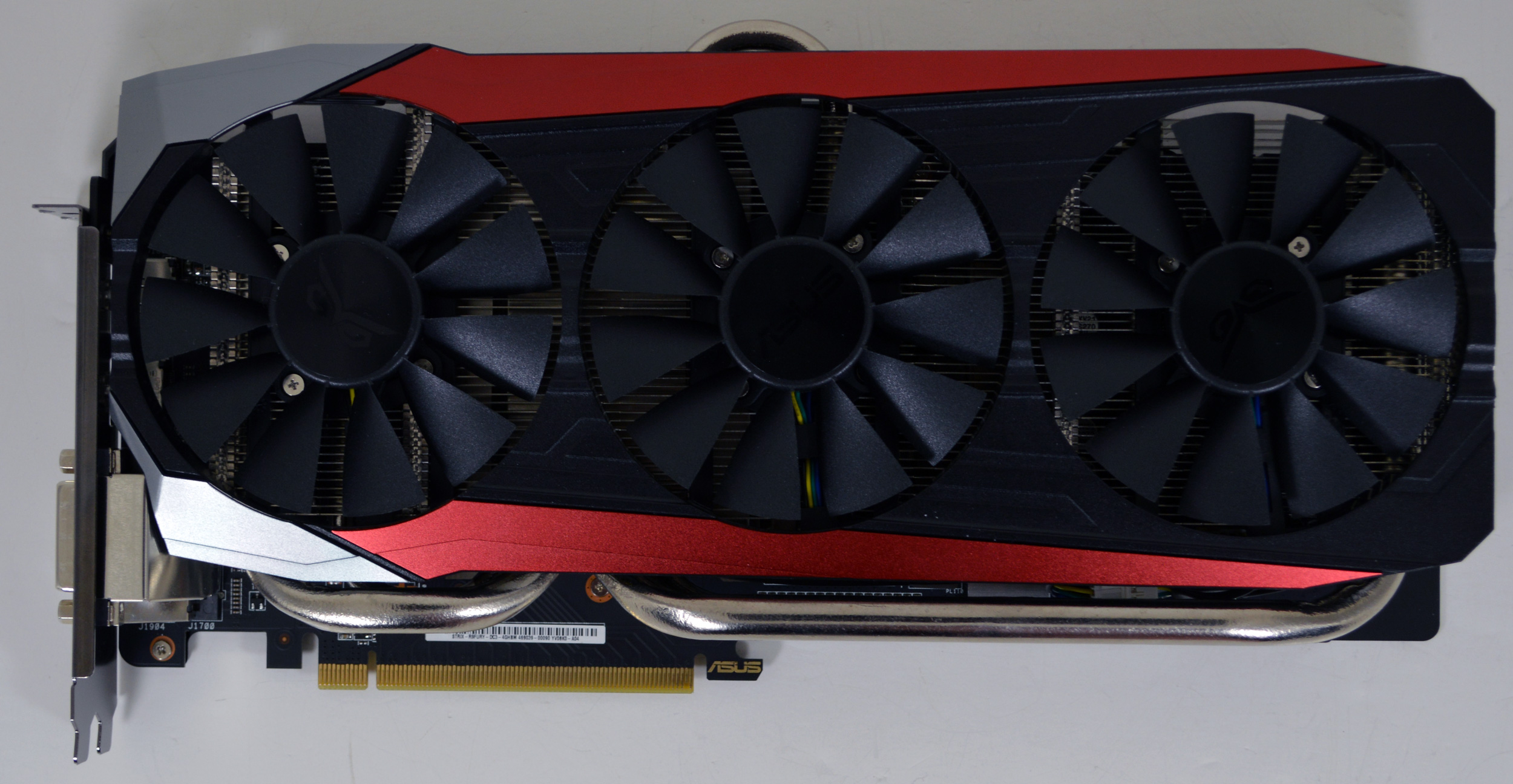
PCB aside, let’s cover the rest of the card. While the PCB is only 10.6” long, ASUS’s DirectCU III cooler is larger yet, slightly overhanging the PCB and extending the total length of the card to 12”. Here ASUS uses a collection of stiffeners, screws, and a backplate to reinforce the card and support the bulky heatsink, giving the resulting card a very sturdy design. In a first for any design we’ve seen thus far, the backplate is actually larger than the card, running the full 12” to match up with the heatsink, and like the Sapphire backplate includes a hole immediately behind the Fiji GPU to allow the many capacitors to better cool. Meanwhile builders with large hands and/or tiny cases will want to make note of the card’s additional height; while the card will fit most cases fine, you may want a magnetic screwdriver to secure the I/O bracket screws, as the additional height doesn’t leave much room for fingers.
For the STRIX ASUS is using one of the company’s triple-fan DirectCU III coolers. Starting at the top of the card with the fans, ASUS calls the fans on this design their “wing-blade” fans. Measuring 90mm in diameter, ASUS tells us that this fan design has been optimized to increase the amount of air pressure on the edge of the fans.
Meanwhile the STRIX also implements ASUS’s variation of zero fan speed idle technology, which the company calls 0dB Fan technology. As one of the first companies to implement zero fan speed idling, the STRIX series has become well known for this feature and the STRIX R9 Fury is no exception. Thanks to the card’s large heatsink ASUS is able to power down the fans entirely while the card is near or at idle, allowing the card to be virtually silent under those scenarios. In our testing this STRIX card has its fans kick in at 55C and shutting off again at 46C.
| ASUS STRIX R9 Fury Zero Fan Idle Points | ||||
| GPU Temperature | Fan Speed | |||
| Turn On | 55C | 28% | ||
| Turn Off | 46C | 25% | ||
As for the DirectCU III heatsink on the STRIX, as one would expect ASUS has gone with a large and very powerful heatsink to cool the Fiji GPU underneath. The aluminum heatsink runs just shy of the full length of the card and features 5 different copper heatpipes, the largest of the two coming in at 10mm in diameter. The heatpipes in turn make almost direct contact with the GPU and HBM, with ASUS having installed a thin heatspeader of sorts to compensate for the uneven nature of the GPU and HBM stacks.
In terms of cooling performance AMD’s Catalyst Control Center reports that ASUS has capped the card at 39% fan speed, though in our experience the card actually tops out at 44%. At this level the card will typically reach 44% by the time it hits 70C, at which point temperatures will rise a bit more before the card reaches homeostasis. We’ve yet to see the card need to ramp past 44%, though if the temperature were to exceed the temperature target we expect that the fans would start to ramp up further. Without overclocking the highest temperature measured was 78C for FurMark, while Crysis 3 topped out at a cooler 71C.
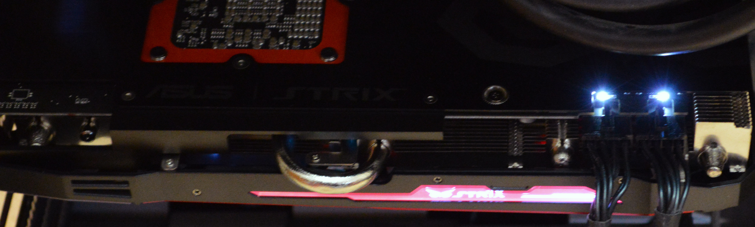
Moving on, ASUS has also adorned the STRIX with a few cosmetic adjustments of their own. The top of the card features a backlit STRIX logo, which pulsates when the card is turned on. And like some prior ASUS cards, there are LEDs next to each of the PCIe power sockets to indicate whether there is a full connection. On that note, with the DirectCU III heatsink extending past the PCIe sockets, ASUS has once again flipped the sockets so that the tabs face the rear of the card, making it easier to plug and unplug the card even with the large heatsink.
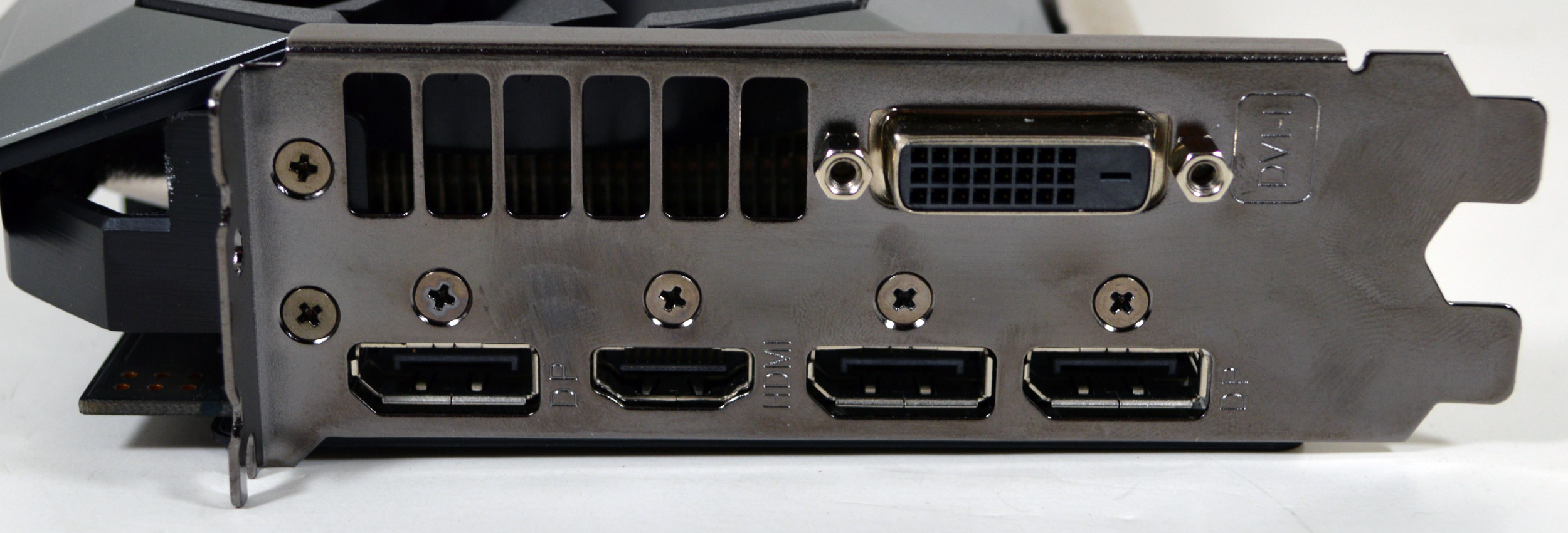
Since this is an ASUS custom PCB, it also means that ASUS has been able to work in their own Display I/O configuration. Unlike the AMD reference PCB, for their custom PCB ASUS has retained a DL-DVI-D port, giving the card a total of 3x DisplayPorts, 1x HDMI port, and 1x DL-DVI-D port. So buyers with DL-DVI monitors not wanting to purchase adapters will want to pay special attention to ASUS’s card.
Finally, on the software front, the STRIX includes the latest iteration of ASUS’s GPU Tweak software, which is now called GPU Tweak II. Since the last time we took at look at GPU Tweak the software has undergone a significant UI overhaul, with ASUS giving it more distinct basic and professional modes. It’s through GPU Tweak II that the card’s OC mode can be accessed, which bumps up the card’s clockspeed to 1020MHz. Meanwhile the other basic overclocking and monitoring functions one would expect from a good overclocking software package are present; GPU Tweak II allows control over clockspeeds, fan speeds, and power targets, while also monitoring all of these features and more.
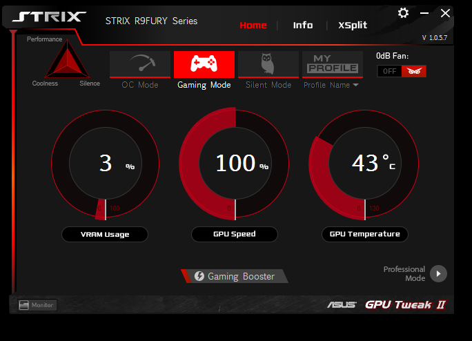


GPU Tweak II also includes a built-in copy of the XSplit game broadcasting software, along with a 1 year premium license. Finally, perhaps the oddest feature of GPU Tweak II is the software’s Gaming Booster feature, which is ASUS’s system optimization utility. Gaming Booster can adjust the system visual effects, system services, and perform memory defragmentation. To be frank, ASUS seems like they were struggling to come up with something to differentiate GPU Tweak II here; messing with system services is a bad idea, and system memory defragmentation is rarely necessary given the nature and abilities of Random Access Memory.
Wrapping things up, the ASUS STRIX R9 Fury will be the most expensive of the R9 Fury launch cards. ASUS is charging a $30 premium for the card, putting the MSRP at $579.


288 Comments
View All Comments
bill.rookard - Friday, July 10, 2015 - link
Impressive results, especially by the Sapphire card. The thing I'm glad to see is that it's such a -quiet- card overall. That bodes well for some of the next releases (I'm dying to see the results of the Nano) and bodes well for AMD overall.Two things I'd like to see:
1) HBM on APU. Even if it were only 1GB or 2GB with an appropriate interface (imaging keeping the 4096 bit interface and either dual or quad-pumping the bus?). The close location of being on-die and high speed of the DRAM would be a very, VERY interesting graphics solution.
2) One would expect that with the cut down on resources, there would have been more of a loss in performance. On average, you see a 7-8% drop in speed after a loss of 13-14% cut in hardware resources and a slight drop in clock speeds. So - where does that mean the bottleneck in the card is? It's possible that something is a bit lopsided internally (it does however perform exceptionally well), so it would be very interesting to tease out the differences to see whats going on inside the card.
mr_tawan - Friday, July 10, 2015 - link
It would be very interesting to run HBM as the system ram instead of DDR on APU. 4GB (for the 1) wouldn't be a lot and may choke on heavy work load, but for casual user (and tablet uses) that's probably enough.It would also allow smaller machine than NUC form factor, I think.
looncraz - Friday, July 10, 2015 - link
HBM wouldn't be terribly well suited for system RAM due to its comparatively low small-read performance and physical form factor. On an APU, for example, it would probably be best used as a single HBM[2] chip on a 1024-bit bus. Probably just 1 or 2GB, largely dedicated to graphics. That is 128GB/s with HBM1 (but 1GB max), 256GB/s with HBM2 (with, IIRC, 4GB max).For a SoC, though, such as the NUC form factor, as you mentioned, it is potentially a game changer only AMD can deliver on x86. Problem is that the net profit margins in that category are quite small, and AMD needs to be chasing higher net margin markets (net margin being a simple result of market volume, share, and product margin).
I'd love to see it, though, for laptops. And with Apple and AMD being friendly, we may end up seeing it. As well as probably seeing it find its way into the next generation of consoles.
Oxford Guy - Saturday, July 11, 2015 - link
Given the high prices Intel is charging for its NUC systems are you really certain it's not profitable? Perhaps sales aren't good because they're overpriced.Stuka87 - Friday, July 10, 2015 - link
The only way to keep the 4096bit bus would be to use four HBM chips, and I highly doubt this would be the case. I am thinking an APU would use either a single HBM chip, or possibly two. The performance boost would still be huge.ajlueke - Friday, July 10, 2015 - link
1) I can't imagine we won't see this. APU scaling with RAM speed was pretty well documented, I would be surprised if there were socket AM4 motherboards that incorporated some amount of HBM directly. Also, AMD performs best against NVidia at 4K, suggesting that Maxwell may be running into a memory bandwidth bottleneck itself. It will be interesting to see how Pascal performs when you couple a die-shrink with the AMD developed HBM2.2) It does suggest that Fiji derives far more benefit from faster clocks versus more resources. That makes the locked down voltages for the Fury X even more glaring. You supply a card that is massively overpowered, with 500W of heat dissipation but no way to increase voltages to really push the clock speed? I hope we get custom BIOS for that card soon.
silverblue - Saturday, July 11, 2015 - link
As regards APU scaling, it's a tough one. More bandwidth is good, however scaling drops above 2133MHz which shows you'd need more hardware to consume it. Would you put in more shaders, or ROPs? I'd go for the latter - don't APUs usually top out at 8 ROPs? Sure, add in more bandwidth, but at the very least, increase how much the APU can actually draw. The HD 4850 had 32 TMUs (like the 7850K) but 16 ROPs, which is double that on offer here.I keep seeing complaints about AMD's ROP count, so perhaps there's some merit to them.
Nagorak - Sunday, July 12, 2015 - link
It's hard to say what the bottleneck is with memory scaling on APUs. It could be something related to the memory controller built into the CPU rather than the GPU not having the resources to benefit.silverblue - Monday, July 13, 2015 - link
Isn't there a 256-bit Radeon Memory Bus link between memory and the GPU? Just a question.Stuka87 - Friday, July 10, 2015 - link
Is it just me, or is the 290X faster now than it used to be when compared to the 980? Perhaps the 15.7 drivers offered some more performance?