The AMD Radeon R9 Fury X Review: Aiming For the Top
by Ryan Smith on July 2, 2015 11:15 AM ESTFiji’s Layout
So what did AMD put in 8.9 billion transistors filling out 596mm2? The answer as it turns out is quite a bit of hardware, though at the same time perhaps not as much (or at least not in the ratios) as everyone was initially hoping for.
The overall logical layout of Fiji is rather close to Hawaii after accounting for the differences in the number of resource blocks and the change in memory. Or perhaps Tonga (R9 285) is the more apt comparison, since that’s AMD’s other GCN 1.2 GPU.
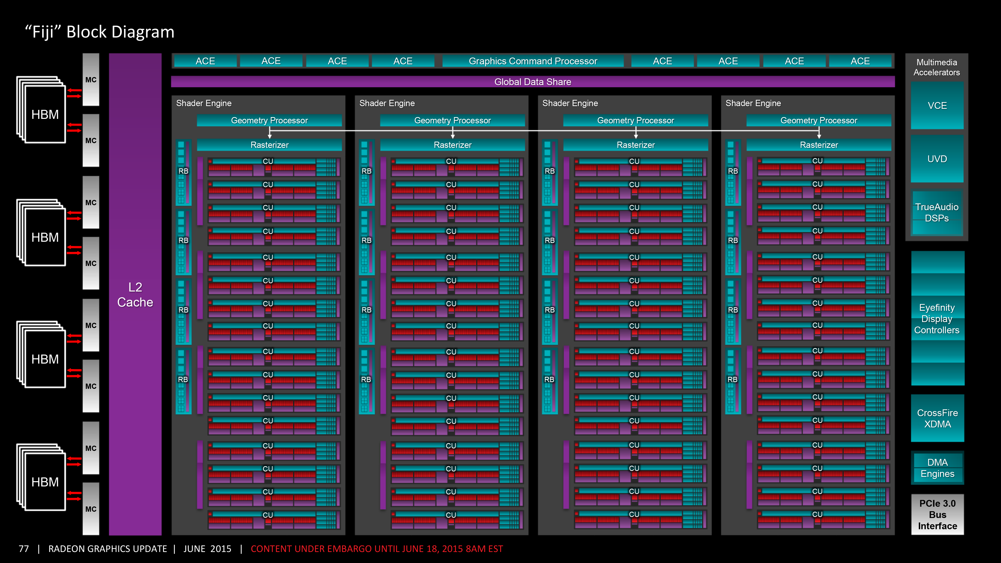
In either case the end result is quite a bit of shading power for Fiji. AMD has bumped up the CU count from 44 to 64, or to put this in terms of the number of ALUs/stream processors, it’s up from 2816 to a nice, round 4096 (2^12). As we discussed earlier FP64 performance has been significantly curtailed in the name of space efficiency, otherwise at Fury X’s stock clockspeed of 1050MHz, you’re looking at enough ALUs to push 8.6 TFLOPs of FP32 operations.
These 64 CUs in turn are laid out in a manner consistent with past GCN designs, with AMD retaining their overall Shader Engine organization. Sub-dividing the GPU into four parts, each shader engine possesses 1 geometry unit, 1 rasterizer unit, 4 render backends (for a total of 16 ROPs), and finally, one-quarter of the CUs, or 16 CUs per shader engine. The CUs in turn continue to be organized in groups of 4, with each group sharing a 16KB L1 scalar cache and 32KB L1 instruction cache. Meanwhile since Fiji’s CU count is once again a multiple of 16, this also does away with Hawaii’s oddball group of 3 CUs at the tail-end of each shader engine.
Looking at the broader picture, what AMD has done relative to Hawaii is to increase the number of CUs per shader engine, but not changing the number of shader engines themselves or the number of other resources available for each shader engine. At the time of the Hawaii launch AMD told us that the GCN 1.1 architecture had a maximum scalability of 4 shader engines, and Fiji’s implementation is consistent with that. While I don’t expect AMD will never go beyond 4 shader engines – there are always changes that can be made to increase scalability – given what we know of GCN 1.1’s limitations, it looks like AMD has not attempted to increase their limits with GCN 1.2. What this means is that Fiji is likely the largest possible implementation of GCN 1.2, with as many resources as the architecture can scale out to without more radical changes under the hood to support more scalability.
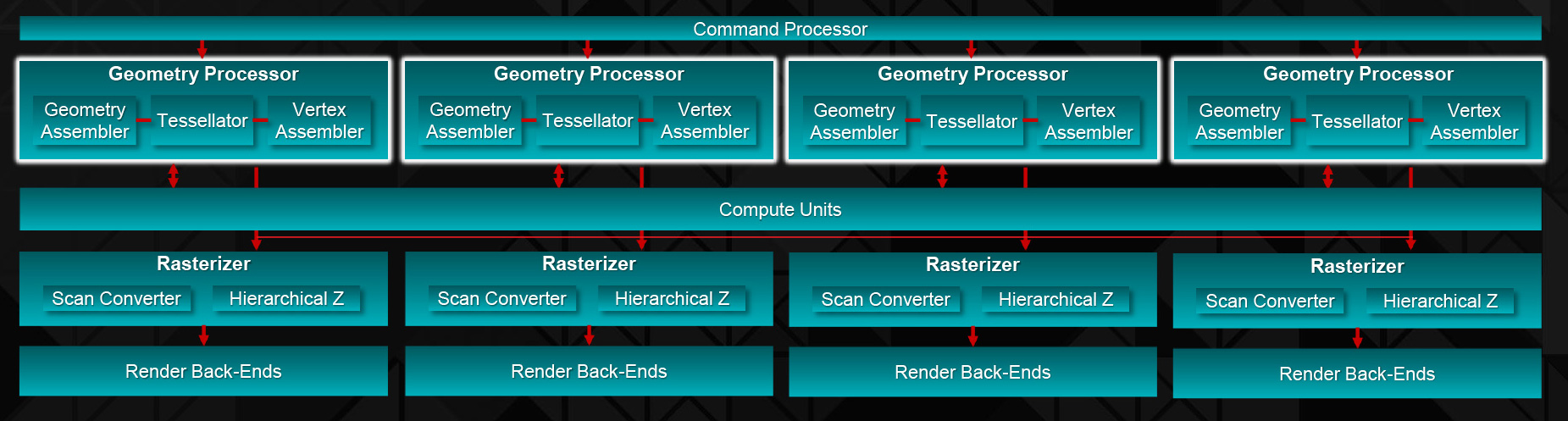
Along those lines, while shading performance is greatly increased over Hawaii, the rest of the front-end is very similar from a raw, theoretical point of view. The geometry processors, which as we mentioned before are organized to 1 per shader engine, just as was the case with Hawaii. With a 1 poly/clock limit here, Fiji has the same theoretical triangle throughput at Hawaii did, with real-world clockspeeds driving things up just a bit over the R9 290X. However as we discussed in our look at the GCN 1.2 architecture, AMD has made some significant under-the-hood changes to the geometry processor design for GCN 1.2/Fiji in order to boost their geometry efficiency, making Fiji’s geometry fornt-end faster and more efficient than Hawaii. As a result the theoretical performance may be unchanged, but in the real world Fiji is going to offer better geometry performance than Hawaii does.
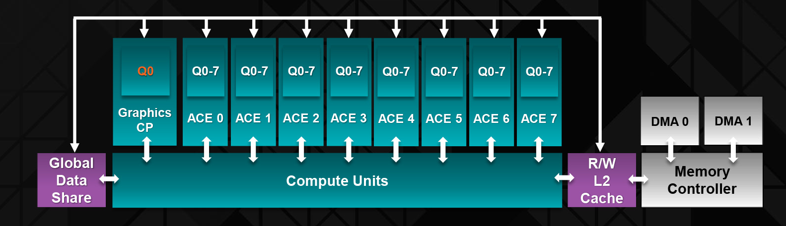
Meanwhile the command processor/ACE structure remains unchanged from Hawaii. We’re still looking at a single graphics command processor paired up with 8 Asynchronous Compute Engines here, and if AMD has made any changes to this beyond what is necessary to support the GCN 1.2 feature set (e.g. context switching, virtualization, and FP16), then they have not disclosed it. AMD is expecting asynchronous shading to be increasingly popular in the coming years, especially in the case of VR, so Fiji’s front-end is well-geared towards the future AMD is planning for.
Moving on, let’s switch gears and talk about the back-end of the processor. There are some significant changes here due to HBM, as to be expected, but there are also some other changes going on as well that are not related to HBM.
Starting with the ROPs, the ROP situation for Fiji remains more or less unchanged from Hawaii. Hawaii shipped with 64 ROPs grouped in to 16 Render Backends (RBs), which at the time AMD told us was the most a 4 shader engine GCN GPU could support. And I suspect that limit is still in play here, leading to Fiji continuing to pack 64 ROPs. Given that AMD just went from 32 to 64 a generation ago, another jump seemed unlikely anyhow (despite earlier rumors to the contrary), but in the end I suspect that AMD had to consider architectural limits just as much as they had to consider performance tradeoffs of more ROPs versus more shaders.
In any case, the real story here isn’t the number of ROPs, but their overall performance. Relative to Hawaii, Fiji’s ROP performance is getting turbocharged for two major reasons. The first is GCN 1.2’s delta color compression, which significantly reduces the amount of memory bandwidth the ROPs consume. Since the ROPs are always memory bandwidth bottlenecked – and this was even more true on Hawaii as the ROP/bandwidth ratio fell relative to Tahiti – anything that reduces memory bandwidth needs can boost performance. We’ve seen this first-hand on R9 285, which with its 256-bit memory bus had no problem keeping up with (and even squeaking past) the 384-bit bus of the R9 280.
The other factor turbocharging Fiji’s ROPs is of course the HBM. In case GCN 1.2’s bandwidth savings were not enough, Fiji also just flat-out has quite a bit more memory bandwidth to play with. The R9 290X and its 5Gbps, 512-bit memory bus offered 320GB/sec, a value that for a GDDR5-based system has only just been overshadowed by the R9 390X. But with Fiji, the HBM configuration as implemented on the R9 Fury X gives AMD 512GB/sec, an increase of 192GB/sec, or 60%.
Now AMD did not just add 60% more memory bandwidth because they felt like it, but because they’re putting that memory bandwidth to good use. The ROPs would still gladly consume it all, and this doesn’t include all of the memory bandwidth consumed by the shaders, the geometry engines, and the other components of the GPU. GPU performance has long outpaced memory bandwidth improvements, and while HBM doesn’t erase any kind of conceptual deficit, it certainly eats into it. With such a significant increase in memory bandwidth and combined with GCN 1.2’s color compression technology, AMD’s effective memory bandwidth to their ROPs has more than doubled from Hawaii to Fiji, which will go a long way towards increasing ROP efficiency and real-world performance. And even if a task doesn’t compress well (e.g. compute) then there’s still 60% more memory bandwidth to work with. Half of a terabyte-per-second of memory bandwidth is simply an incredible amount to have for such a large pool of VRAM, since prior to this only GPU caches operated that quickly.
Speaking of caches, Fiji’s L2 cache has been upgraded as well. With Hawaii AMD shipped a 1MB cache, and now with Fiji that cache has been upgraded again to 2MB. Even with the increase in memory bandwidth, going to VRAM is still a relatively expensive operation, so trying to stay on-cache is beneficial up to a point, which is why AMD spent the additional transistors here to double the L2 cache. Both AMD and NVIDIA have gone with relatively large L2 caches in this latest round, and with their latest generation color compression technologies it makes a lot of sense; since the L2 cache can store color-compressed tiles, all of a sudden L2 caches are a good deal more useful and worth the space they consume.
Finally, we’ll get to HBM in a more detail in a bit, but let’s take a quick look at the HBM controller layout. With Fiji there are 8 HBM memory controllers, and each HBM controller in turn drives one-half of an HBM stack, meaning 2 controllers are necessary to drive a full stack. And while AMD’s logical diagram doesn’t illustrate it, Fiji is almost certainly wired such that each HBM memory controller is tightly coupled with 8 ROPs and 256KB of L2 cache. AMD has not announced any future Fiji products with less than 4GB of VRAM, so we’re not expecting any parts with disabled ROPs, but if they did that would give you an idea of how things would be disabled.


458 Comments
View All Comments
TallestJon96 - Saturday, July 4, 2015 - link
This card is not the disappointment people make it out to be. One month ago this card would have been a MASSIVE success. What is strange to me is that they didn't reduce price, even slightly to compete with the new 980 ti. I suspect it was to avoid a price war, but I would say at $600 this card is attractive, but at $650 you only really want it for water cooling. I suspect the price will drop more quickly than the 980 ti.mccoy3 - Saturday, July 4, 2015 - link
So it is as expensive as the 980Ti by delivering less performance and requires watercooling. Once Nvidia settles for a TITAN Y including HBM, its all over for the red guys.just4U - Saturday, July 4, 2015 - link
Well that would be great news for AMD though wouldn't it since Nvidia would have to pay for the use of HBM in some form or another..Oxford Guy - Saturday, July 4, 2015 - link
AMD could have released a hot leaf blower like the GTX 480 and chose not to.chizow - Monday, July 6, 2015 - link
No, they couldn't have. Fury X is already a 275W and that's with the benefit of low temp leakage using a WC *AND* the benefit of a self-professed 15-20W TDP surplus from HBM. That means in order for Fury X to still fall 10% short of 980Ti, it is already using 25+20W, so 45W more power.Their CUSTOM cooled 7/8th cut Fury is going to be 275W typical board power as well and its cut down, so yeah the difference in functional unit power is most likely going to be the same as the difference in thermal leakage due to operating temperatures between water and custom air cooling. A hot leaf blower, especially one as poor as AMD's reference would only be able to cool a 6/8 cut Fiji or lower, but at that point you might as well get a Hawaii based card.
Oxford Guy - Thursday, July 9, 2015 - link
Your posts don't even try to sound sane. I wrote about the GTX 480, which was designed to run hot and loud. Nvidia also couldn't release a fully-enabled chip.Ignore the point about the low-grade cooler on the 480 which ran hot and was very loud.
Ignore the point about the card being set to run hot, which hurt performance per watt (see this article if you don't get it).
How much is Nvidia paying you to astroturf? Whatever it is, it's too much.
Margalus - Monday, July 6, 2015 - link
this AMD card pumps out more heat than any NVidia card. Just because it runs a tad cooler with water cooling doesn't mean the heat is not there. It's just removed faster with water cooling, but the heat is still generated and the card will blow out a lot more hot air into the room than any NVidia card.Oxford Guy - Friday, July 10, 2015 - link
If you can't afford AC then stick with something like a 750 Ti. Otherwise the extra heat is hardly a big deal.zodiacfml - Saturday, July 4, 2015 - link
My excitement with HBM has subsided as I realized that this is too costly to be implemented in AMD's APUs even next year. Yet, I hope they do as soon as possible even if it would mean HBM on a narrower bus.jburns - Saturday, July 4, 2015 - link
Probably the best graphics card review I've ever read! Detailed and balanced... Thanks Ryan for an excellent review.