AMD Dives Deep On High Bandwidth Memory - What Will HBM Bring AMD?
by Ryan Smith on May 19, 2015 8:40 AM ESTHistory: Where GDDR5 Reaches Its Limits
To really understand HBM we’d have to go all the way back to the first computer memory interfaces, but in the interest of expediency and sanity, we’ll condense that lesson down to the following. The history of computer and memory interfaces is a consistent cycle of moving between wide parallel interfaces and fast serial interfaces. Serial ports and parallel ports, USB 2.0 and USB 3.1 (Type-C), SDRAM and RDRAM, there is a continual process of developing faster interfaces, then developing wider interfaces, and switching back and forth between them as conditions call for.
So far in the race for PC memory, the pendulum has swung far in the direction of serial interfaces. Though 4 generations of GDDR, memory designers have continued to ramp up clockspeeds in order to increase available memory bandwidth, culminating in GDDR5 and its blistering 7Gbps+ per pin data rate. GDDR5 in turn has been with us on the high-end for almost 7 years now, longer than any previous memory technology, and in the process has gone farther and faster than initially planned.
But in the cycle of interfaces, the pendulum has finally reached its apex for serial interfaces when it comes to GDDR5. Back in 2011 at an AMD video card launch I asked then-graphics CTO Eric Demers about what happens after GDDR5, and while he expected GDDR5 to continue on for some time, it was also clear that GDDR5 was approaching its limits. High speed buses bring with them a number of engineering challenges, and while there is still headroom left on the table to do even better, the question arises of whether it’s worth it.

AMD 2011 Technical Forum and Exhibition
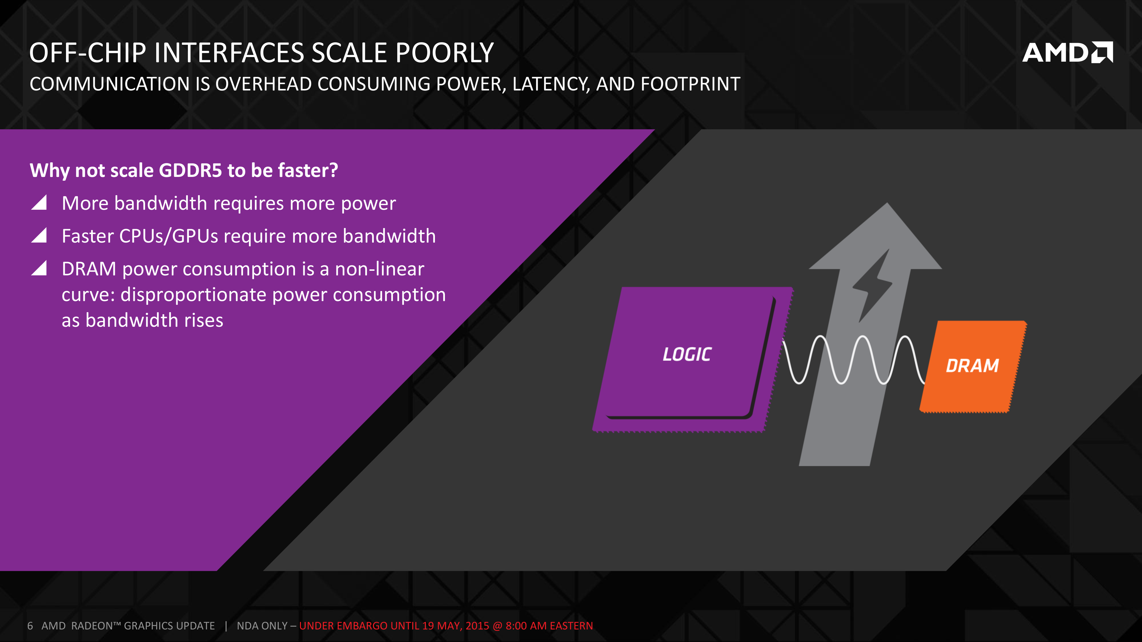
The short answer in the minds of the GPU community is no. GDDR5-like memories could be pushed farther, both with existing GDDR5 and theoretical differential I/O based memories (think USB/PCIe buses, but for memory), however doing so would come at the cost of great power consumption. In fact even existing GDDR5 implementations already draw quite a bit of power; thanks to the complicated clocking mechanisms of GDDR5, a lot of memory power is spent merely on distributing and maintaining GDDR5’s high clockspeeds. Any future GDDR5-like technology would only ratchet up the problem, along with introducing new complexities such as a need to add more logic to memory chips, a somewhat painful combination as logic and dense memory are difficult to fab together.
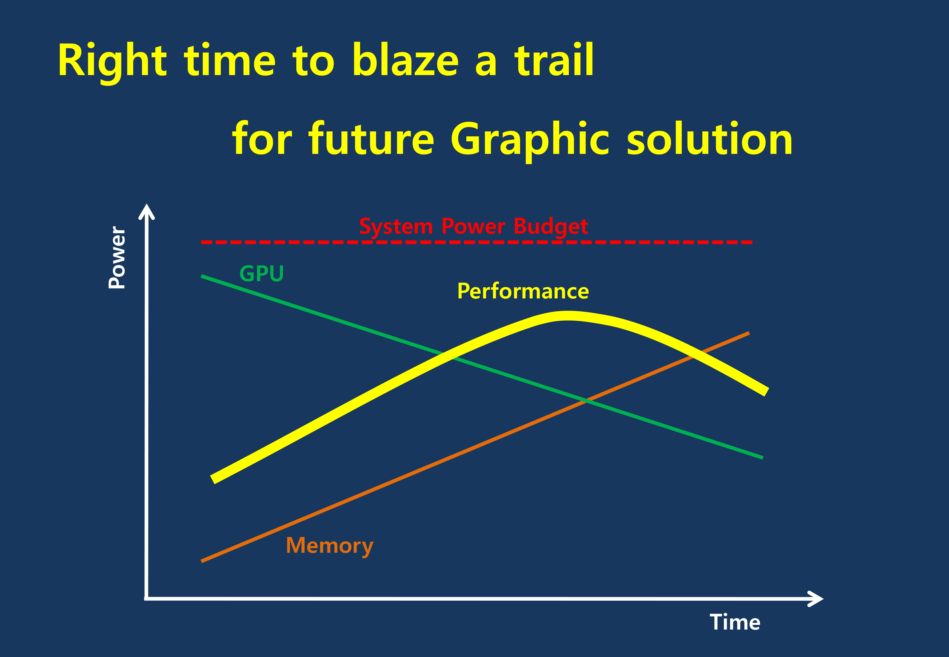
The current GDDR5 power consumption situation is such that by AMD’s estimate 15-20% of Radeon R9 290X’s (250W TDP) power consumption is for memory. This being even after the company went with a wider, slower 512-bit GDDR5 memory bus clocked at 5GHz as to better contain power consumption. So using a further, faster, higher power drain memory standard would only serve to exacerbate that problem.
All the while power consumption for consumer devices has been on a downward slope as consumers (and engineers) have made power consumption an increasingly important issue. The mobile space, with its fixed battery capacity, is of course the prime example, but even in the PC space power consumption for CPUs and GPUs has peaked and since come down some. The trend is towards more energy efficient devices – the idle power consumption of a 2005 high-end GPU would be intolerable in 2015 – and that throws yet another wrench into faster serial memory technologies, as power consumption would be going up exactly at the same time as overall power consumption is expected to come down, and individual devices get lower power limits to work with as a result.
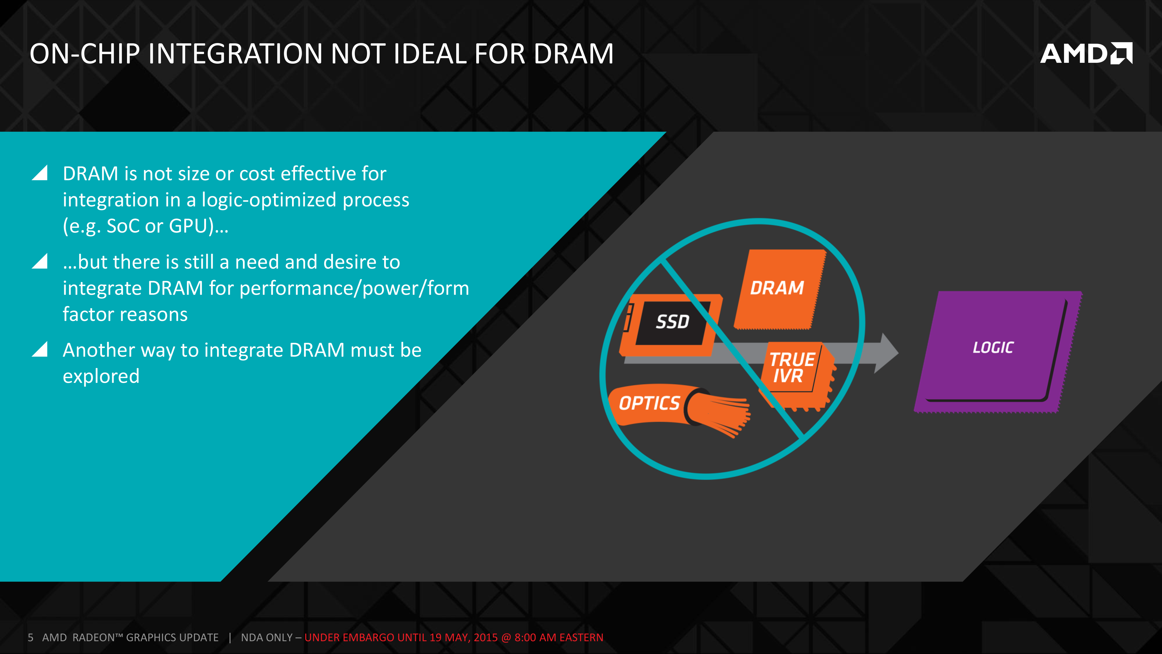
Finally, coupled with all of the above has been issues with scalability. We’ll get into this more when discussing the benefits of HBM, but in a nutshell GDDR5 also ends up taking a lot of space, especially when we’re talking about 384-bit and 512-bit configurations for current high-end video cards. At a time when everything is getting smaller, there is also a need to further miniaturize memory, something that GDDR5 and potential derivatives wouldn’t be well suited to resolve.
The end result is that in the GPU memory space, the pendulum has started to swing back towards parallel memory interfaces. GDDR5 has been taken to the point where going any further would be increasingly inefficient, leading to researchers and engineers looking for a wider next-generation memory interface. This is what has led them to HBM.


163 Comments
View All Comments
chizow - Tuesday, May 19, 2015 - link
Nice article Ryan, I think this gets back to some of the general tech deep dives that a lot of people miss on AT, rather than the obligatory item reviews that I know you guys have to put out as well. Always interesting to read about new and upcoming technology, thanks for the read!This part I think however, on last page needs to be clarified, as it is REALLY important to stay consistent in terminology now that GPU socket and PCB topology is changing:
"By AMD’s own estimate, a single HBM-equipped GPU package would be less than 70mm X 70mm (4900mm2), versus 110mm X 90mm (9900mm2) for R9 290X."
Even by AMD's own slide, that is *PCB area* occupied by either the HBM GPU package, or the GPU + GDDR5 modules. Calling everything a "package" doesn't really fit here and just confuses the issue if we keep the term Package intact, meaning GPU substrate sitting on PCB.
extide - Tuesday, May 19, 2015 - link
No, package is the correct term, as it is a single complete item that attaches to the PCB, including the GPU, RAM, interposer, etc all in one piece. It is not much different than the MCM (Multi Chip Modules) that many manufacturers (Intel for example) have used in the past. Since the memory is all on the package, the PCB area used is the same size as the package itself, in this case.chizow - Tuesday, May 19, 2015 - link
I agree the HBM package terminology is correct, but I'm not referring to that. I'm referring to the reference that the 290X package size is 110mm x 90mm for R9 290X. That's not very clear, because they are counting the *PCB AREA* on the 290X and using it synonymously with Package.It would be more clearly stated if it read something like:
"By AMD’s own estimate, the PCB area occupied by a single HBM-equipped GPU package would be less than 70mm X 70mm (4900mm2), versus 110mm X 90mm (9900mm2) PCB area for R9 290X that includes the GPU package and GDDR5 modules."
gamerk2 - Tuesday, May 19, 2015 - link
How much does the production of the Interposer cost? It's obviously going to eat into AMDs margins, which would imply that unless they sell more product, their profits will actually decline. Likewise, I wonder if that extra cost is going to squeeze them on the low end, where they currently have an advantage.extide - Tuesday, May 19, 2015 - link
Probably on the order of $10/GPU -- not a ton, but enough to be a significant item on the BoM.DanNeely - Tuesday, May 19, 2015 - link
I doubt gen 1 HBM will show up on budget cards; and wouldn't hold my breath on gen 2 or 3 either. For the 4xx generation, they're only putting it on the 490 family. 460-480 are going to remain at GDDR5. HBM will presumably kill off GDDR5 for midlevel cards over the next few years; but unless it becomes as cheap as DDR4 it's not going to be a factor on budget GPUs.SunLord - Tuesday, May 19, 2015 - link
I wonder how this will impact dual gpu cardsKevin G - Tuesday, May 19, 2015 - link
It'd actually make the board design simpler as difficult part, the memory traces, are now all in the interposer. The challenge for a dual GPU designs shifts toward power and cooling.With the board area savings, they could conceptually do a triple GPU card. The problem wouldn't be the designs of such a card but actually getting enough power. Of course they could go out of the PCIe spec and go towards a 525W design for such a triple GPU beast.
testbug00 - Tuesday, May 19, 2015 - link
Naw, they would go for a full water cooled 725W card XD (1W under the electric limits of PCI + 8 + 8 pin iirc) trollololoolololol.don't think anyone would do a triple GPU card for consumers. The scaling is still pretty bad beyond 2 iirc.
Kevin G - Tuesday, May 19, 2015 - link
The wonderful thing about having all the GPUs on a single board is that incorporating a private high speed bus between chips becomes possible to improve scaling. AMD attempted this before with the 4870X2: http://www.anandtech.com/show/2584/3However, it was never really utilized as it was disabled via drivers.
Alternatively, multiple GPU dies and memory could just be placed onto the same the interposer. Having a fast and wide bus between GPU dies would then become trivial. Power consumption and more importantly power density, would not be so trivial.