AMD Dives Deep On High Bandwidth Memory - What Will HBM Bring AMD?
by Ryan Smith on May 19, 2015 8:40 AM ESTHistory: Where GDDR5 Reaches Its Limits
To really understand HBM we’d have to go all the way back to the first computer memory interfaces, but in the interest of expediency and sanity, we’ll condense that lesson down to the following. The history of computer and memory interfaces is a consistent cycle of moving between wide parallel interfaces and fast serial interfaces. Serial ports and parallel ports, USB 2.0 and USB 3.1 (Type-C), SDRAM and RDRAM, there is a continual process of developing faster interfaces, then developing wider interfaces, and switching back and forth between them as conditions call for.
So far in the race for PC memory, the pendulum has swung far in the direction of serial interfaces. Though 4 generations of GDDR, memory designers have continued to ramp up clockspeeds in order to increase available memory bandwidth, culminating in GDDR5 and its blistering 7Gbps+ per pin data rate. GDDR5 in turn has been with us on the high-end for almost 7 years now, longer than any previous memory technology, and in the process has gone farther and faster than initially planned.
But in the cycle of interfaces, the pendulum has finally reached its apex for serial interfaces when it comes to GDDR5. Back in 2011 at an AMD video card launch I asked then-graphics CTO Eric Demers about what happens after GDDR5, and while he expected GDDR5 to continue on for some time, it was also clear that GDDR5 was approaching its limits. High speed buses bring with them a number of engineering challenges, and while there is still headroom left on the table to do even better, the question arises of whether it’s worth it.

AMD 2011 Technical Forum and Exhibition
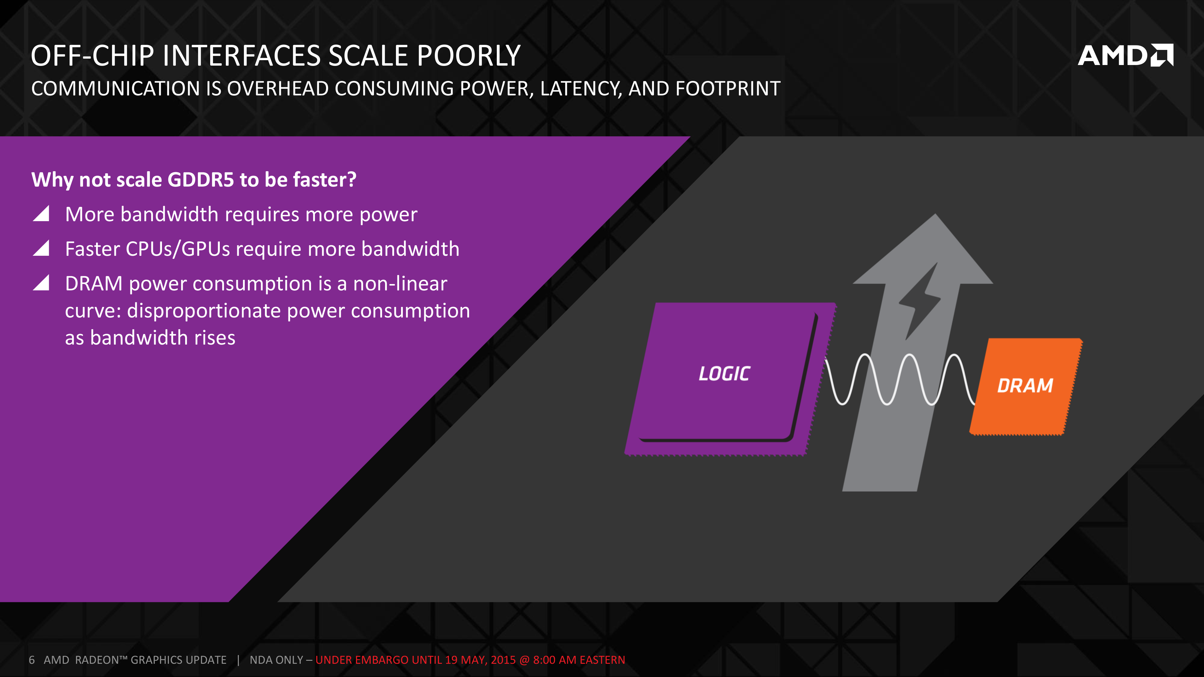
The short answer in the minds of the GPU community is no. GDDR5-like memories could be pushed farther, both with existing GDDR5 and theoretical differential I/O based memories (think USB/PCIe buses, but for memory), however doing so would come at the cost of great power consumption. In fact even existing GDDR5 implementations already draw quite a bit of power; thanks to the complicated clocking mechanisms of GDDR5, a lot of memory power is spent merely on distributing and maintaining GDDR5’s high clockspeeds. Any future GDDR5-like technology would only ratchet up the problem, along with introducing new complexities such as a need to add more logic to memory chips, a somewhat painful combination as logic and dense memory are difficult to fab together.
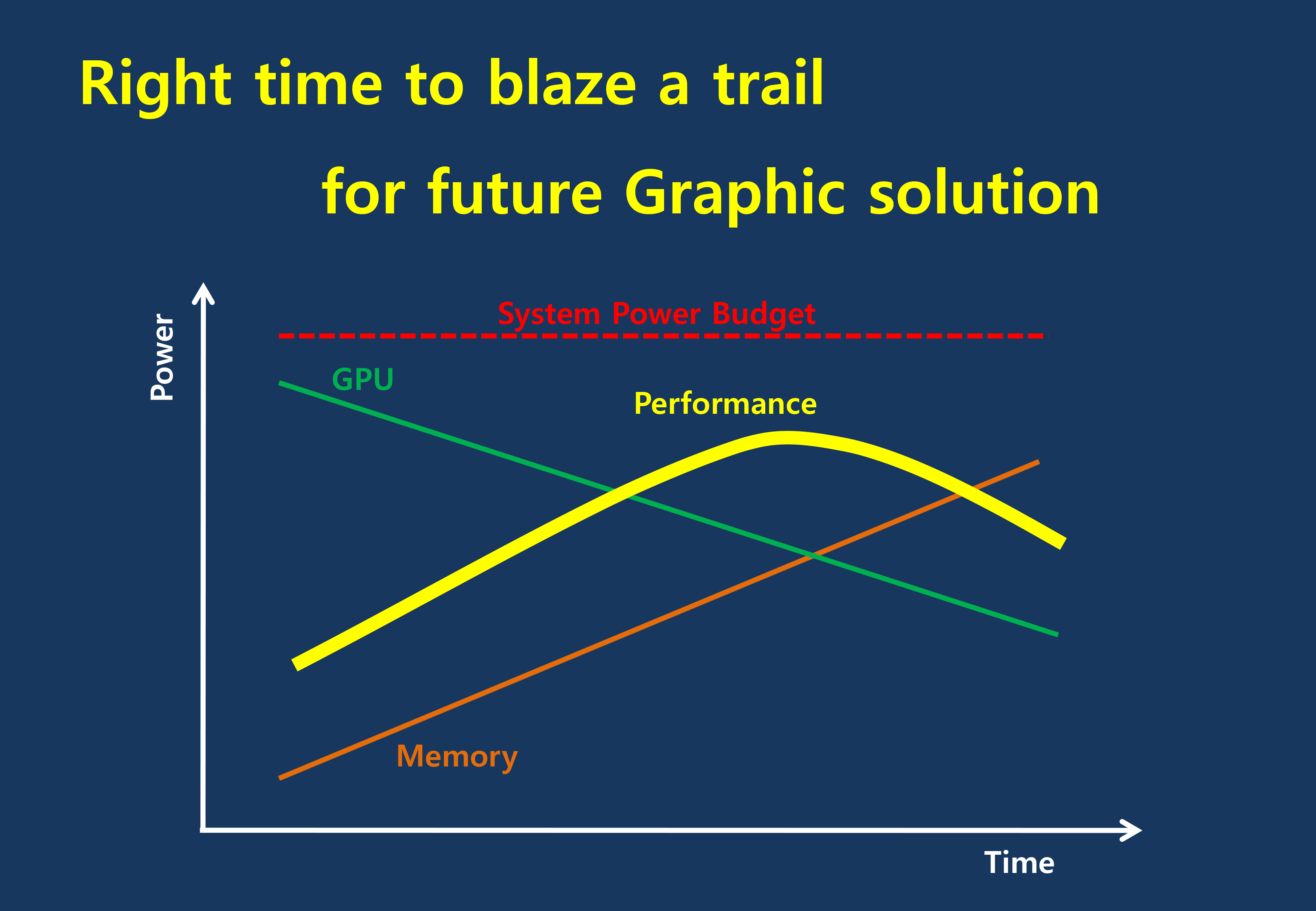
The current GDDR5 power consumption situation is such that by AMD’s estimate 15-20% of Radeon R9 290X’s (250W TDP) power consumption is for memory. This being even after the company went with a wider, slower 512-bit GDDR5 memory bus clocked at 5GHz as to better contain power consumption. So using a further, faster, higher power drain memory standard would only serve to exacerbate that problem.
All the while power consumption for consumer devices has been on a downward slope as consumers (and engineers) have made power consumption an increasingly important issue. The mobile space, with its fixed battery capacity, is of course the prime example, but even in the PC space power consumption for CPUs and GPUs has peaked and since come down some. The trend is towards more energy efficient devices – the idle power consumption of a 2005 high-end GPU would be intolerable in 2015 – and that throws yet another wrench into faster serial memory technologies, as power consumption would be going up exactly at the same time as overall power consumption is expected to come down, and individual devices get lower power limits to work with as a result.
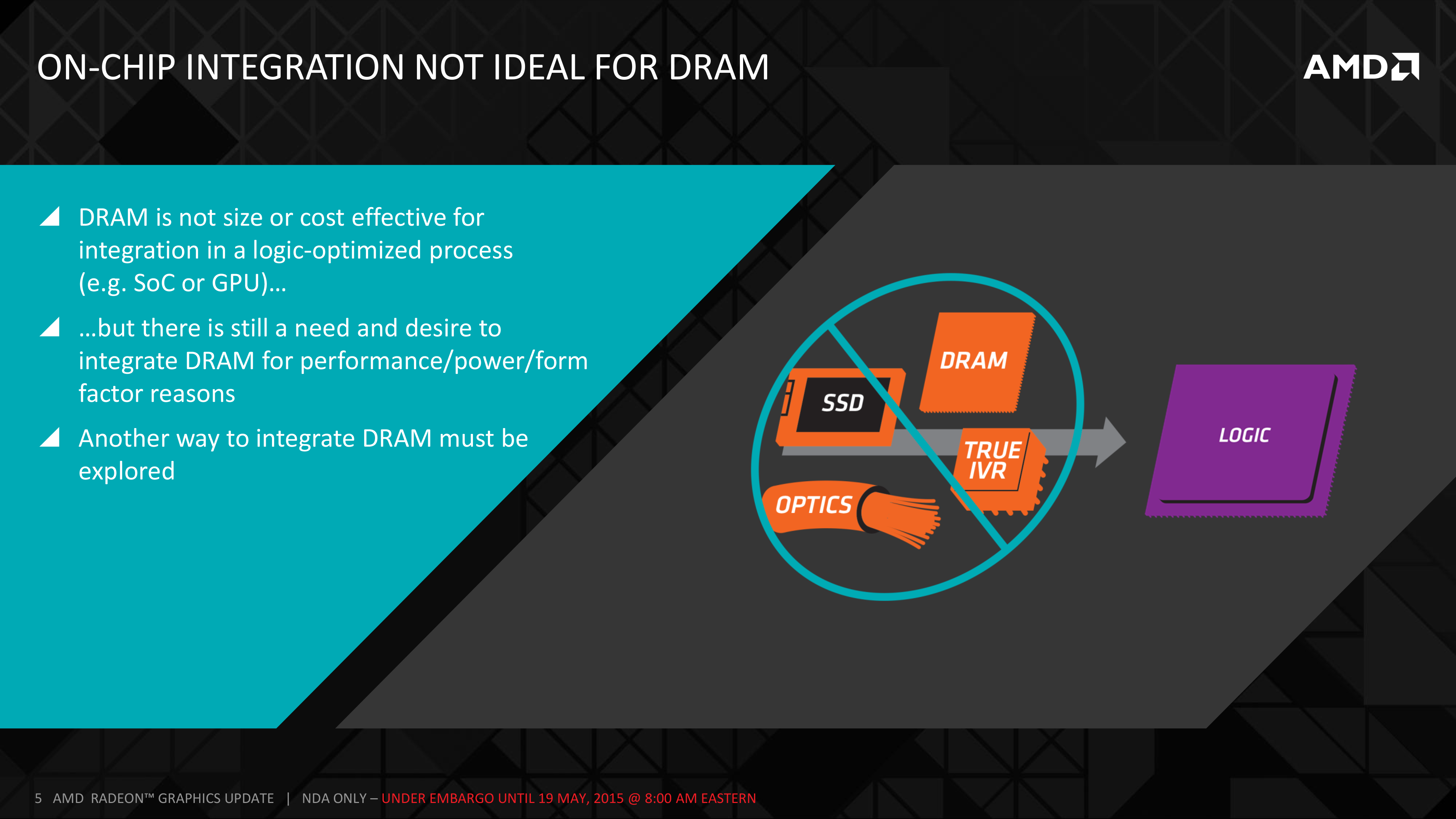
Finally, coupled with all of the above has been issues with scalability. We’ll get into this more when discussing the benefits of HBM, but in a nutshell GDDR5 also ends up taking a lot of space, especially when we’re talking about 384-bit and 512-bit configurations for current high-end video cards. At a time when everything is getting smaller, there is also a need to further miniaturize memory, something that GDDR5 and potential derivatives wouldn’t be well suited to resolve.
The end result is that in the GPU memory space, the pendulum has started to swing back towards parallel memory interfaces. GDDR5 has been taken to the point where going any further would be increasingly inefficient, leading to researchers and engineers looking for a wider next-generation memory interface. This is what has led them to HBM.


163 Comments
View All Comments
chizow - Wednesday, May 20, 2015 - link
lol @ trollranger101 doing what he does best, nothing.at80eighty - Thursday, May 21, 2015 - link
check any thread - he is predictable.chizow - Thursday, May 21, 2015 - link
Yes, predictably clearing up, refuting, and debunking the misinformation spread by...you guessed it. AMD fanboys like yourselves.Intel999 - Tuesday, May 19, 2015 - link
AMD has six months exclusivity on HBM1 since they co created it with Hynix. That is why no one else is using it yet.chizow - Wednesday, May 20, 2015 - link
Possibly, would make sense, and also explain why they are still going forward with it even if the 1st iteration isn't exactly optimal due to covered limitations (4GB, increased costs etc)SunLord - Tuesday, May 19, 2015 - link
HBM2 is supposed to double the bandwidth and density so 8GB of ram and 1TB/sec.... for a 4 chip setup it also seems to allow upto 32GB but HBM2 it isn't supposed to be ready till Q2 2016Kevin G - Tuesday, May 19, 2015 - link
Which is fine as the big 16/14 nm FinFET next generation chips aren't due to till around then anyway. The memory technology and foundry plans are aligning rather well.testbug00 - Tuesday, May 19, 2015 - link
Appears HBM2 increase it from 1GB to up to 4GB (2-4GB).Page 12:
http://www.hotchips.org/wp-content/uploads/hc_arch...
hans_ober - Tuesday, May 19, 2015 - link
How does temperature affect TSV's and the silicon interposer? Continuous thermal cycling usually stresses out joints. Wouldn't want one of the many thousand joints to break.Mr Perfect - Tuesday, May 19, 2015 - link
If I understand it correctly, joints usually suffer from thermal cycling because they are between different materials that heat and cool at different rates. The TSVs will be connecting silicon to silicon, so presumably the heating and cooling will be uniform and not stress the joints in that way.