AMD Dives Deep On High Bandwidth Memory - What Will HBM Bring AMD?
by Ryan Smith on May 19, 2015 8:40 AM ESTHistory: Where GDDR5 Reaches Its Limits
To really understand HBM we’d have to go all the way back to the first computer memory interfaces, but in the interest of expediency and sanity, we’ll condense that lesson down to the following. The history of computer and memory interfaces is a consistent cycle of moving between wide parallel interfaces and fast serial interfaces. Serial ports and parallel ports, USB 2.0 and USB 3.1 (Type-C), SDRAM and RDRAM, there is a continual process of developing faster interfaces, then developing wider interfaces, and switching back and forth between them as conditions call for.
So far in the race for PC memory, the pendulum has swung far in the direction of serial interfaces. Though 4 generations of GDDR, memory designers have continued to ramp up clockspeeds in order to increase available memory bandwidth, culminating in GDDR5 and its blistering 7Gbps+ per pin data rate. GDDR5 in turn has been with us on the high-end for almost 7 years now, longer than any previous memory technology, and in the process has gone farther and faster than initially planned.
But in the cycle of interfaces, the pendulum has finally reached its apex for serial interfaces when it comes to GDDR5. Back in 2011 at an AMD video card launch I asked then-graphics CTO Eric Demers about what happens after GDDR5, and while he expected GDDR5 to continue on for some time, it was also clear that GDDR5 was approaching its limits. High speed buses bring with them a number of engineering challenges, and while there is still headroom left on the table to do even better, the question arises of whether it’s worth it.

AMD 2011 Technical Forum and Exhibition
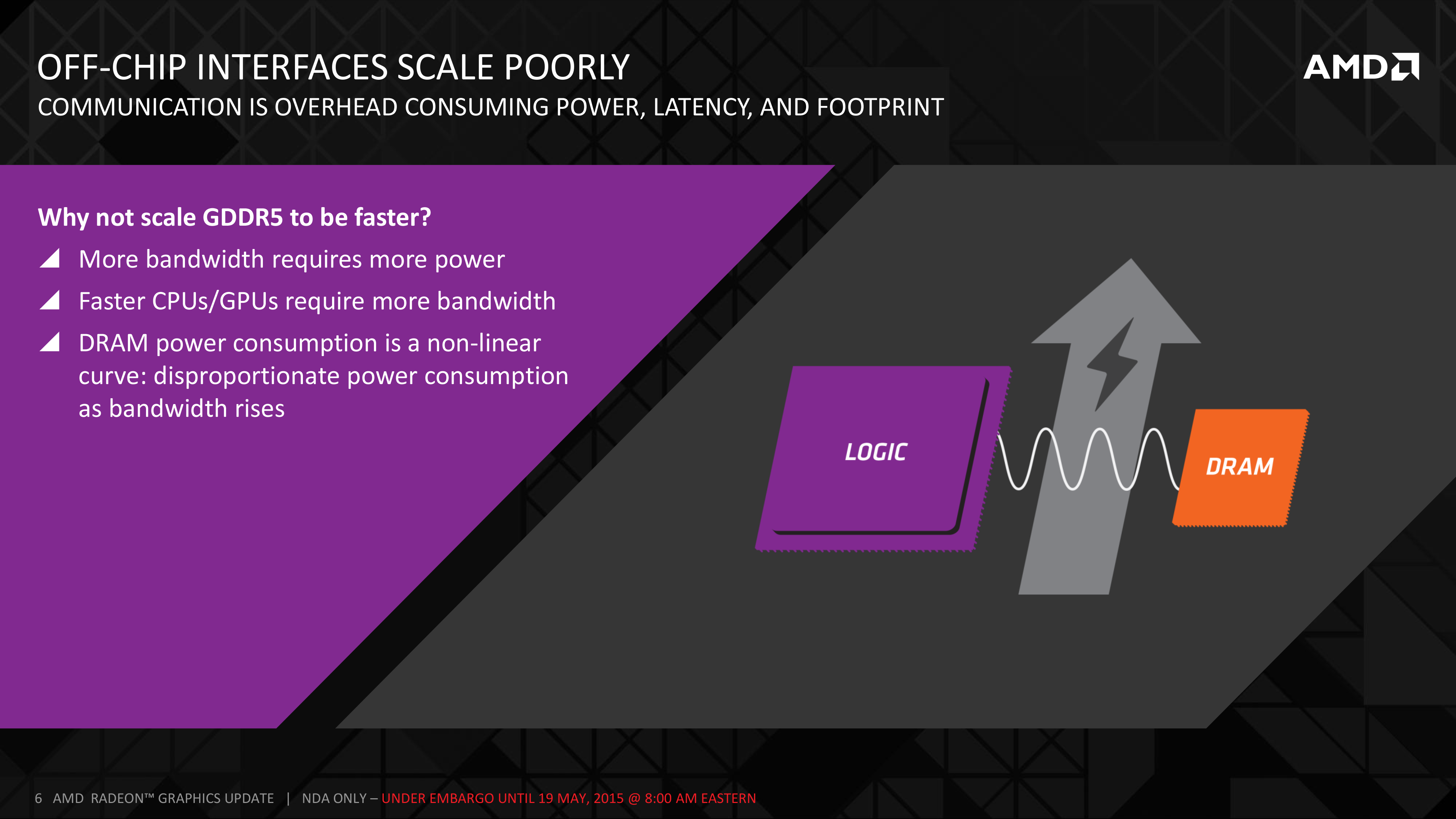
The short answer in the minds of the GPU community is no. GDDR5-like memories could be pushed farther, both with existing GDDR5 and theoretical differential I/O based memories (think USB/PCIe buses, but for memory), however doing so would come at the cost of great power consumption. In fact even existing GDDR5 implementations already draw quite a bit of power; thanks to the complicated clocking mechanisms of GDDR5, a lot of memory power is spent merely on distributing and maintaining GDDR5’s high clockspeeds. Any future GDDR5-like technology would only ratchet up the problem, along with introducing new complexities such as a need to add more logic to memory chips, a somewhat painful combination as logic and dense memory are difficult to fab together.
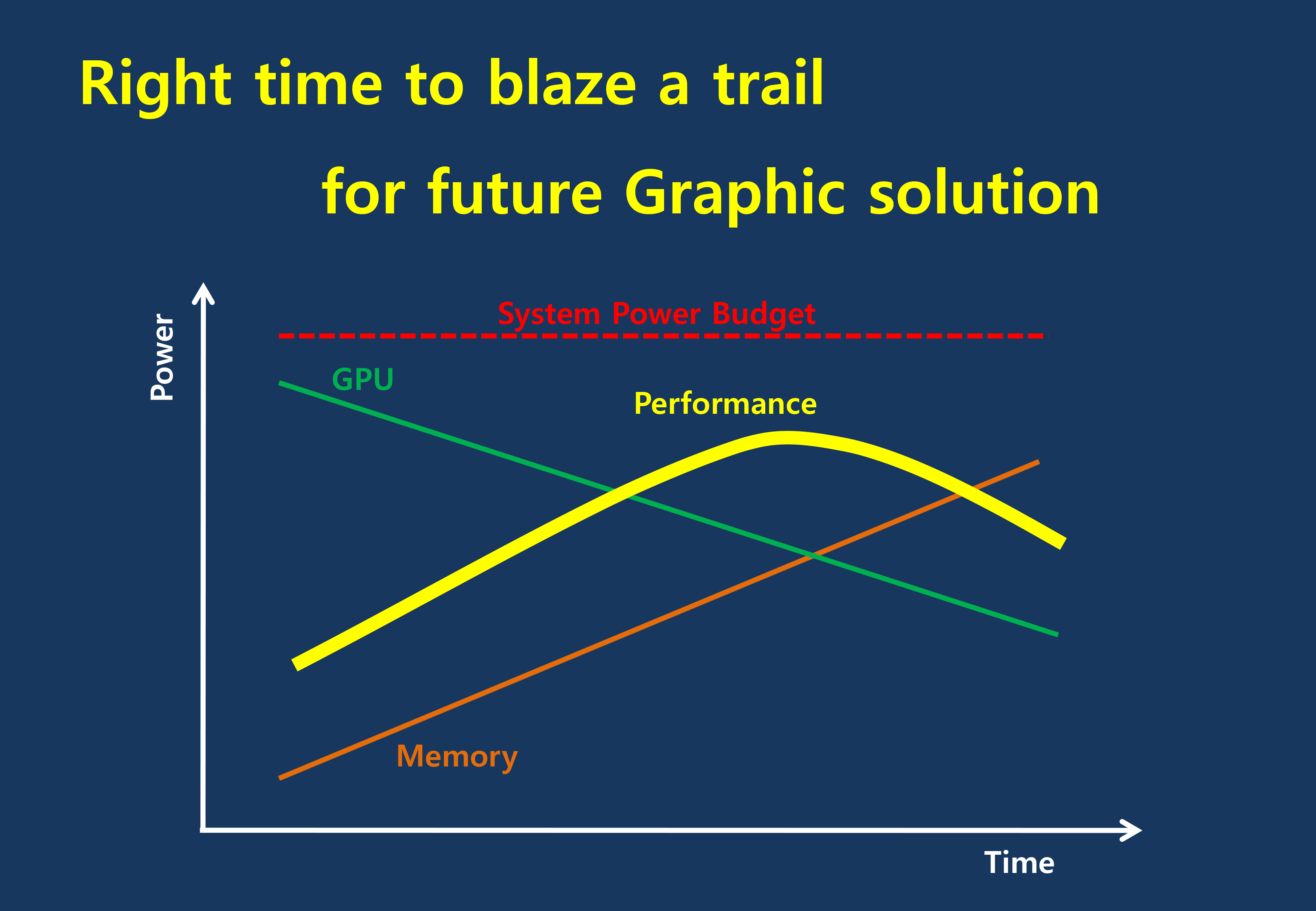
The current GDDR5 power consumption situation is such that by AMD’s estimate 15-20% of Radeon R9 290X’s (250W TDP) power consumption is for memory. This being even after the company went with a wider, slower 512-bit GDDR5 memory bus clocked at 5GHz as to better contain power consumption. So using a further, faster, higher power drain memory standard would only serve to exacerbate that problem.
All the while power consumption for consumer devices has been on a downward slope as consumers (and engineers) have made power consumption an increasingly important issue. The mobile space, with its fixed battery capacity, is of course the prime example, but even in the PC space power consumption for CPUs and GPUs has peaked and since come down some. The trend is towards more energy efficient devices – the idle power consumption of a 2005 high-end GPU would be intolerable in 2015 – and that throws yet another wrench into faster serial memory technologies, as power consumption would be going up exactly at the same time as overall power consumption is expected to come down, and individual devices get lower power limits to work with as a result.
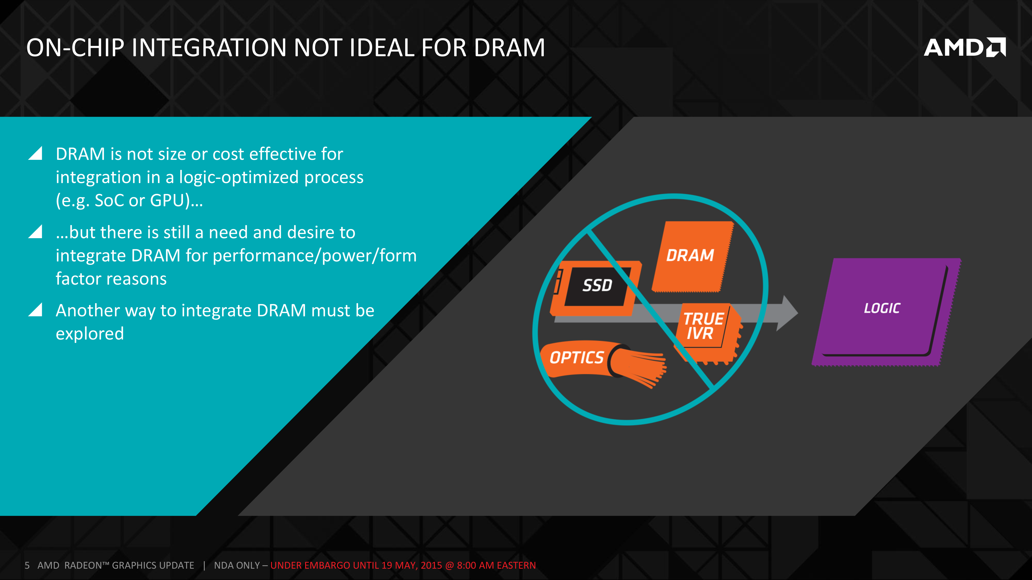
Finally, coupled with all of the above has been issues with scalability. We’ll get into this more when discussing the benefits of HBM, but in a nutshell GDDR5 also ends up taking a lot of space, especially when we’re talking about 384-bit and 512-bit configurations for current high-end video cards. At a time when everything is getting smaller, there is also a need to further miniaturize memory, something that GDDR5 and potential derivatives wouldn’t be well suited to resolve.
The end result is that in the GPU memory space, the pendulum has started to swing back towards parallel memory interfaces. GDDR5 has been taken to the point where going any further would be increasingly inefficient, leading to researchers and engineers looking for a wider next-generation memory interface. This is what has led them to HBM.


163 Comments
View All Comments
akamateau - Thursday, May 28, 2015 - link
You miss the whole point.DX12 solves Witcher.
HBM was designed to manage the high volume of drawcalls that DX12 enables.
ALL GPU's were crippled with DX11. DX11 is DEAD.
You can't render an object until you draw it. Dx11 does not support multicore or multithreaded cpu processing of graphics, DX12 does.
With DX12 ALL CPU cores feed the GPU.
akamateau - Monday, June 8, 2015 - link
If AMD can put 4-8 gigs of HBM on a GPU then they can do the same with CPU's as well as APU's. All of the Patents that I am showing below reference 3d statcked memoryIn fact one interesting quote from the patents listed below is this:
"Packaging chips in closer proximity not only improves performance, but can also reduce the energy expended when communicating between the processor and memory. It would be desirable to utilize the large amount of "empty" silicon that is available in an interposer."
AMD has plans to fill that empty silicon with much more memory.
The point: REPLACE SYSTEM DYNAMIC RAM WITH ON-DIE HBM 2 OR 3!
Eliminating the electrical path distance to a few millimeters from 4-8 centimeters would be worth a couple of clocks of latency. If AMD is building HBM and HBM 2 then they are also building HBM 3 or more!
Imagine what 64gb of HBM could do for a massive server die such as Zen? The energy savings alone would be worth it never mind the hugely reduced motherboard size, eliminating sockets and RAM packaging. The increased amount of CPU's/blade or mobo also reduces costs as servers can become much more dense.
Most folks now only run 4-8 gigs in their laptops or desktops. Eliminating DRAM and replacing it with HBM is a huge energy and mechanical savings as well as a staggering performance jump and it destroys DDR5. That process will be very mature in a year and costs will drop. Right now the retail cost of DRAM per GB is about $10. Subtract packaging and channel costs and that drops to $5 or less. Adding 4-8 GB of HBM has a very cheap material cost, likely the main expense is the process, testing and yields. Balance that against the energy savings MOBO real estate savings and HBM replacing system DRAM becomes even more likely without the massive leap in performance as an added benefit.
The physical cost savings is quite likely equivalent to the added process cost. Since Fiji will likely be released at a very competitive price point.
AMD is planning on replacing system DRAM memory with stacked HBM. Here are the Patents. They are all published last year and this year with the same inventor; Gabriel H. Loh and the assignee is of course AMD.
Stacked memory device with metadata management
WO 2014025676 A1
"Memory bandwidth and latency are significant performance bottlenecks in many processing systems. These performance factors may be improved to a degree through the use of stacked, or three-dimensional (3D), memory, which provides increased bandwidth and reduced intra-device latency through the use of through-silicon vias (TSVs) to interconnect multiple stacked layers of memory. However, system memory and other large-scale memory typically are implemented as separate from the other components of the system. A system implementing 3D stacked memory therefore can continue to be bandwidth-limited due to the bandwidth of the interconnect connecting the 3D stacked memory to the other components and latency-limited due to the propagation delay of the signaling traversing the relatively-long interconnect and the handshaking process needed to conduct such signaling. The inter-device bandwidth and inter-device latency have a particular impact on processing efficiency and power consumption of the system when a performed task requires multiple accesses to the 3D stacked memory as each access requires a back-and-forth communication between the 3D stacked memory and thus the inter-device bandwidth and latency penalties are incurred twice for each access."
Interposer having embedded memory controller circuitry
US 20140089609 A1
" For high-performance computing systems, it is desirable for the processor and memory modules to be located within close proximity for faster communication (high bandwidth). Packaging chips in closer proximity not only improves performance, but can also reduce the energy expended when communicating between the processor and memory. It would be desirable to utilize the large amount of "empty" silicon that is available in an interposer. "
Die-stacked memory device with reconfigurable logic
US 8922243 B2
"Memory system performance enhancements conventionally are implemented in hard-coded silicon in system components separate from the memory, such as in processor dies and chipset dies. This hard-coded approach limits system flexibility as the implementation of additional or different memory performance features requires redesigning the logic, which design costs and production costs, as well as limits the broad mass-market appeal of the resulting component. Some system designers attempt to introduce flexibility into processing systems by incorporating a separate reconfigurable chip (e.g., a commercially-available FPGA) in the system design. However, this approach increases the cost, complexity, and size of the system as the system-level design must accommodate for the additional chip. Moreover, this approach relies on the board-level or system-level links to the memory, and thus the separate reconfigurable chip's access to the memory may be limited by the bandwidth available on these links."
Hybrid cache
US 20140181387 A1
"Die-stacking technology enables multiple layers of Dynamic Random Access Memory (DRAM) to be integrated with single or multicore processors. Die-stacking technologies provide a way to tightly integrate multiple disparate silicon die with high-bandwidth, low-latency interconnects. The implementation could involve vertical stacking as illustrated in FIG. 1A, in which a plurality of DRAM layers 100 are stacked above a multicore processor 102. Alternately, as illustrated in FIG. 1B, a horizontal stacking of the DRAM 100 and the processor 102 can be achieved on an interposer 104. In either case the processor 102 (or each core thereof) is provided with a high bandwidth, low-latency path to the stacked memory 100.
Computer systems typically include a processing unit, a main memory and one or more cache memories. A cache memory is a high-speed memory that acts as a buffer between the processor and the main memory. Although smaller than the main memory, the cache memory typically has appreciably faster access time than the main memory. Memory subsystem performance can be increased by storing the most commonly used data in smaller but faster cache memories."
Partitionable data bus
US 20150026511 A1
"Die-stacked memory devices can be combined with one or more processing units (e.g., Central Processing Units (CPUs), Graphics Processing Units (GPUs), and Accelerated Processing Units (APUs)) in the same electronics package. A characteristic of this type of package is that it can include, for example, over 1000 data connections (e.g., pins) between the one or more processing units and the die-stacked memory device. This high number of data connections is significantly greater than data connections associated with off-chip memory devices, which typically have 32 or 64 data connections."
Non-uniform memory-aware cache management
US 20120311269 A1
"Computer systems may include different instances and/or kinds of main memory storage with different performance characteristics. For example, a given microprocessor may be able to access memory that is integrated directly on top of the processor (e.g., 3D stacked memory integration), interposer-based integrated memory, multi-chip module (MCM) memory, conventional main memory on a motherboard, and/or other types of memory. In different systems, such system memories may be connected directly to a processing chip, associated with other chips in a multi-socket system, and/or coupled to the processor in other configurations.
Because different memories may be implemented with different technologies and/or in different places in the system, a given processor may experience different performance characteristics (e.g., latency, bandwidth, power consumption, etc.) when accessing different memories. For example, a processor may be able to access a portion of memory that is integrated onto that processor using stacked dynamic random access memory (DRAM) technology with less latency and/or more bandwidth than it may a different portion of memory that is located off-chip (e.g., on the motherboard). As used herein, a performance characteristic refers to any observable performance measure of executing a memory access operation."
“NoC Architectures for Silicon Interposer Systems Why pay for more wires when you can get them (from your interposer) for free?” Natalie Enright Jerger, Ajaykumar Kannan, Zimo Li Edward S. Rogers Department of Electrical and Computer Engineering University of Toronto Gabriel H. Loh AMD Research Advanced Micro Devices, Inc”
http://www.eecg.toronto.edu/~enright/micro14-inter...
“3D-Stacked Memory Architectures for Multi-Core Processors” Gabriel H. Loh Georgia Institute of Technology College of Computing”
http://ag-rs-www.informatik.uni-kl.de/publications...
“Efficiently Enabling Conventional Block Sizes for Very Large Die-stacked DRAM Caches” Gabriel H. Loh⋆ Mark D. Hill†⋆ ⋆ AMD Research † Department of Computer Sciences Advanced Micro Devices, Inc. University of Wisconsin – Madison”
http://research.cs.wisc.edu/multifacet/papers/micr...
All of this adds up to HBM being placed on-die as a replacement of or maybe supplement to system memory. But why have system DRAM if you can build much wider bandwidth memory closer to the CPU on-die? Unless of course you build socketed HBM DRAM and a completely new system memory bus to feed it.
Replacing system DRAM memory with on-die HBM has the same benefits for the performance and energy demand of the system as it has for GPU's. Also it makes for smaller motherboards, no memory sockets and no memory packaging.
Of course this is all speculation. But it also makes sense.
amilayajr - Tuesday, June 16, 2015 - link
With HBM in mind. Does AMD holds the patent for this? Is Nvidia just going to use HBM for free? Any one care to elaborate ? Because if Nvidia gets to use it for free then that's really funny for AMD side considering they are the one who research it and developed it. Am I making sense?