AMD Dives Deep On High Bandwidth Memory - What Will HBM Bring AMD?
by Ryan Smith on May 19, 2015 8:40 AM EST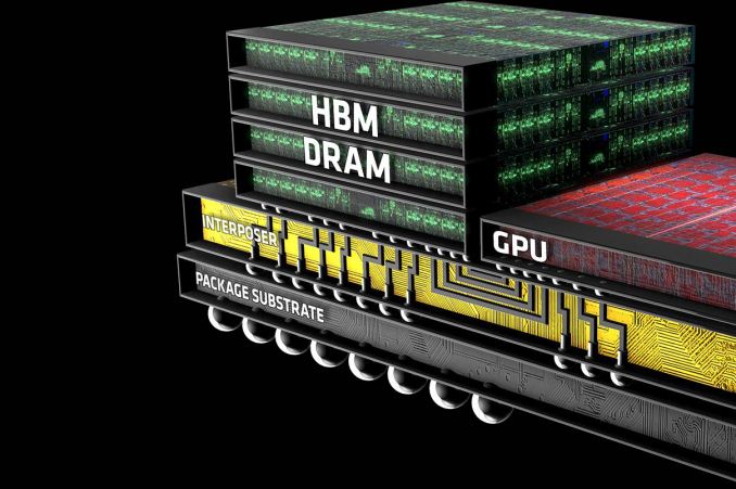
Though it didn’t garner much attention at the time, in 2011 AMD and memory manufacturer Hynix (now SK Hynix) publicly announced plans to work together on the development and deployment of a next generation memory standard: High Bandwidth Memory (HBM). Essentially pitched as the successor to GDDR, HBM would implement some very significant changes in the working of memory in order to further improve memory bandwidth and turn back the dial on memory power consumption.
AMD (and graphics predecessor ATI) for their part have in the last decade been on the cutting edge of adopting new memory technologies in the graphics space, being the first to deploy products based on the last 2 graphics DDR standards, GDDR4, and GDDR5. Consequently, AMD and Hynix’s announcement, though not a big deal at the time, was a logical extension of AMD’s past behavior in continuing to explore new memory technologies for future products. Assuming everything were to go well for the AMD and Hynix coalition – something that was likely, but not necessarily a given – in a few years the two companies would be able to bring the technology to market.
AMD Financial Analyst Day 2015
It’s now 4 years later, and successful experimentation has given way to productization. Earlier this month at AMD’s 2015 Financial Analyst day, the company announced that they would be releasing their first HBM-equipped GPU – the world’s first HBM-equipped GPU, in fact – to the retail market this quarter. Since then there have been a number of questions of just what AMD intends to do with HBM and just what it means for their products (is it as big of a deal as it seems?), and while AMD is not yet ready to reveal the details of their forthcoming HBM-equipped GPU, the company is looking to hit the ground running on HBM in order to explain what the technology is and what it can do for their products ahead of the GPU launch later that quarter.
To date there have been a number of presentations released on HBM, including by memory manufactures, the JEDEC groups responsible for shaping HBM, AMD, and even NVIDIA. So although the first HBM products have yet to hit retail shelves, the underpinnings of HBM are well understood, at least inside of engineering circles. In fact it’s the fact that HBM is really only well understood within those technical circles that’s driving AMD’s latest disclosure today. AMD sees HBM as a significant competitive advantage over the next year, and with existing HBM presentations having been geared towards engineers, academia, and investors, AMD is looking to take the next step and reach out to end-users about HBM technology.
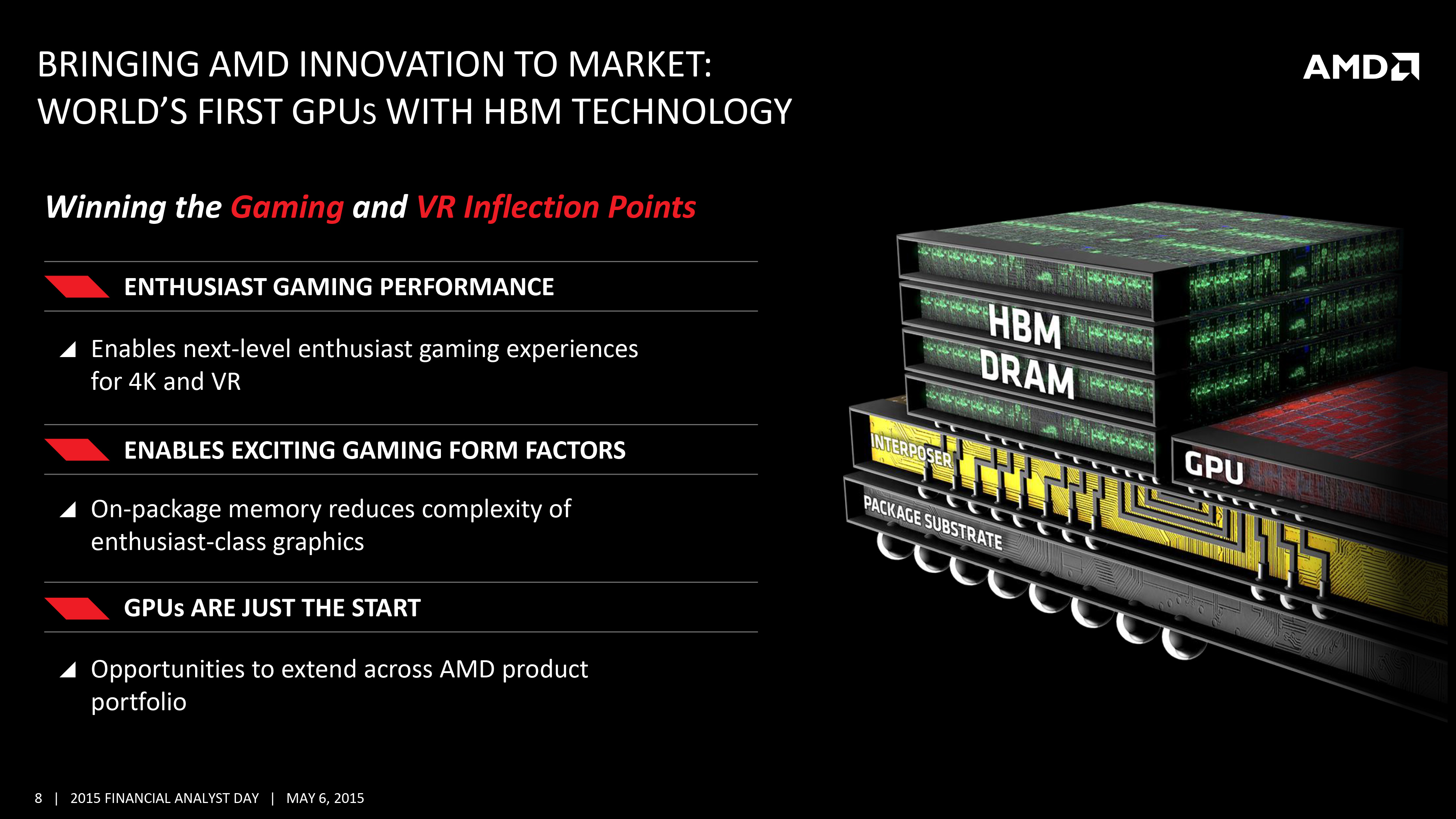
This brings us to the topic of today’s article: AMD’s deep dive disclosure on High Bandwidth Memory. Looking to set the stage ahead of their next GPU launch, AMD is reaching out to technical and gaming press to get the word out about HBM and what it means for AMD’s products. Ideally for AMD, an early disclosure on HBM can help to drum up interest in their forthcoming GPU before it launches later this quarter, but if nothing else it can help answer some burning questions about what to expect ahead of the launch. So with that in mind, let’s dive in.
I'd also like to throw out a quick thank you to AMD Product CTO and Corporate Fellow Joe Macri, who fielded far too many questions about HBM.


163 Comments
View All Comments
jjj - Tuesday, May 19, 2015 - link
"First part of the solution to that in turn was to develop something capable of greater density routing, and that something was the silicon interposer. ""Moving on, the other major technological breakthrough here is the creation of through-silicon vias (TSVs). "
You guys are acting like interposers and TSV were created by AMD and Hynix for this, it's hugely misleading the way you chose to phrase things.
And ofc, as always when you do this kind of article (Aptina, Synaptics, Logitech and a few more in the last few years), it's more advertising than anything else.You don't talk about other similar technologies ,existing or potential, you just glorify the one you are presenting.
Crunchy005 - Tuesday, May 19, 2015 - link
This isn't an article on HBM itself but AMDs next gen cards. They are focusing on AMD becasue of that fact. If this were about HBM itself i'm sure they would talk about other technologies out their as well. Don't criticize because they are staying on topic in the article.testbug00 - Tuesday, May 19, 2015 - link
a side note for the article, ATI also was the main developer of GDDR3, with JEDEC helping a little. Nvidia launched with it first, but, ATI __DID__ most of the design work.testbug00 - Tuesday, May 19, 2015 - link
Having finished the article, I was also under the impression that high clock GDDR5 used 2-2.5 watts per chip on the board. I don't see what 7GBps GDDR5 with 50% more chips would use only 5% more power. (currently on graph 290 == 16 chips @5GBps, ~30W. Titan X = 24 chips @7GBps, ~31.5W).Given AMD's ~15-20% for the 290x, I would put that at around 35-50W, while NVidia's solution is at least 50W. Of course, I could be wrong!
testbug00 - Tuesday, May 19, 2015 - link
As a note, I get that you used the GDDR5 bandwidth/W you can get... However, that's likely at the best point in the pref/watt curve. I suspect that's under 5GBps, based on AMD's claimed GDDR5 consumption on the 290(X) and their memory clock.Which, would put AMD's under that number, and, NVidia's further under that number.
testbug00 - Tuesday, May 19, 2015 - link
Oh, and, here the slide you have that "proves" it: http://images.anandtech.com/doci/9266/HBM_9_Compar...That means at 7GBps, at max bandwidth/watt, the Titan X should be using ~63 watts of power (28/10.66) * 24 = 63.04
Ryan Smith - Tuesday, May 19, 2015 - link
They're rough estimates based on power consumption per bit of bandwidth and should be taken as such. Titan X has more chips, but it doesn't have to drive a wider memory bus.HighTech4US - Tuesday, May 19, 2015 - link
Facts have never gotten in the way of testbug's anti-Nvidia drivel.testbug00 - Tuesday, May 19, 2015 - link
So, should I assume that GDDR5 chips don't use power if you don't make a wider bus? And that 7GBps is the best Bandwidth/watt of GDDR5? Or that GDDR5 power consumption doesn't change when you raise or lower the clockspeed?Nvidia's generalized power is just easier to calculate because they use 7GBps. Anyhow, my guesstimations for the 290x is that it uses is 32W given perfect power scaling from 5GBps to 7GBps and that it has less chips to run voltage.
The reality is probably AMD's is 40-50W and NVidia is 50-60W. Running more GDDR5 chips at higher clockspeeds, even on a smaller bus, should result in higher power usage.
I have rose tinted glasses, I also do have a brain.
silverblue - Tuesday, May 19, 2015 - link
It's quite the role-reversal, really. Back in the GT 200 days, NVIDIA were throwing out cards with wider memory buses, and AMD showed them that it was (mostly) unnecessary.Whichever solution uses the most power for GDDR5 stands to gain the most with a move to HBM. I'd be interested in seeing how much juice the memory on a 12GB card uses...