The Intel Haswell-E X99 Motherboard Roundup with ASUS, GIGABYTE, ASRock and MSI
by Ian Cutress on September 25, 2014 11:30 AM ESTGIGABYTE X99: The New
Similar to ASUS, GIGABYTE comes to X99 with a few new features to tantalize the taste buds of potential users. All new features tend to fall into two categories: improving the underlying product or adding functionality. GIGABYTE is going for a bit of column A and a bit from column B in X99, although we still see stalwarts of the Ultra Durable line as well as upgraded audio.
GIGABYTE’s first major addition to X99 is its use of gold in the connectors. Typically a motherboard manufacturer selects which socket they want from the socket manufacturer (either LOTES or FOXCONN usually) for their motherboards. If the motherboard manufacturer wants something different, then a price is arranged. One of the main components of a socket price above the base is the coating on the pins themselves. Motherboard manufacturers typically use 5-micron gold tipped connections to create a fine line between the copper and the outside world which reduces corrosion and increases the longevity of the device over multiple insertions. For X99, GIGABYTE is using six times the amount of gold in the socket and all PCIe/DRAM connection points:
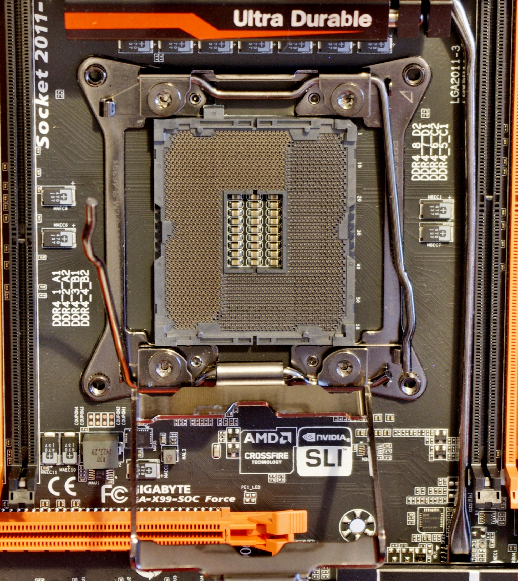
Technically a thicker coating also affords less resistance for the current to travel through due to the increased diameter, although I question whether this makes a sizable difference on this scale. As long as the user does not accidentally bend a pin in the socket, the main benefit will be for users who are in humid environments and do not use all the PCIe/DRAM slots in their motherboard. I am sure there might be a small benefit to GIGABYTE on returns as well, although I assume the return rate based on corrosion is relatively low.
The next feature is one that benefits anyone who has ever put a PC together. With screwdriver in hand, sometimes placing the motherboard screws in can be a bit of an issue, especially when the screwdriver slips out of the screw head and decides to plunge full force into the delicate components on the motherboard. GIGABYTE has decided to implement an expanded area around each screw hole on the motherboard to make this less of an issue:
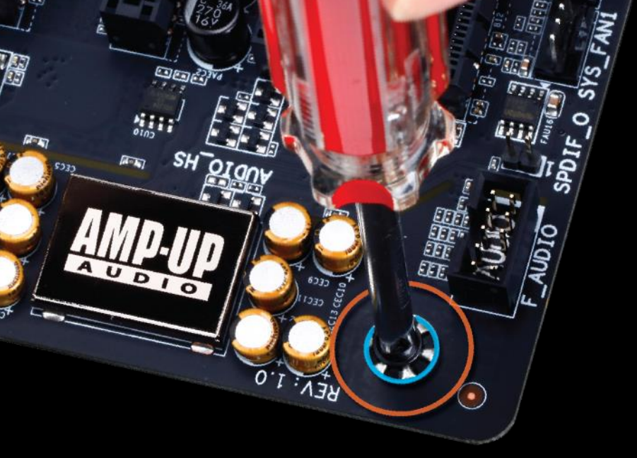
The blue area is where the standard screw mounting hole is, and the orange area is GIGABYTE’s new mounting exclusion zone. These circles are not on the board but the area around each screw hole is definitely free from extra transistors that might get removed by some clumsy hands:
Some of these have printed white text around, but the idea is to at least remove most of the transistors out of the immediate vicinity. I have the unfortunate circumstance of actually being clumsy enough to take a transistor off of one of these motherboards in this review, although for that particular motherboard it did not matter much. If that motherboard had this modification, I probably would not have taken anything off. But there is a lot of if in that statement. Nevertheless, it is an interesting feature to have.
One of the interesting discussions about PCIe bandwidth and X99, aside from the 28 or 40 PCIe lanes debacle depending on which CPU you have, is the one regarding three and four-way GPU setups. Nominally, Intel’s default setting allows x16/x16/x8 for three way, and by using switches this can be expanded to x8/x8/x8/x8 for four-way. But ultimately in this configuration we have lost eight lanes of bandwidth. This is because the CPU essentially has a limited about of PEG lanes it can support with its own clocks, and to get the full x16/x8/x8/x8 scenario, motherboard manufacturers must introduce their own external clock sources. This costs money, so not all manufacturers will do it, however GIGABYTE seems committed to this across its entire product stack:
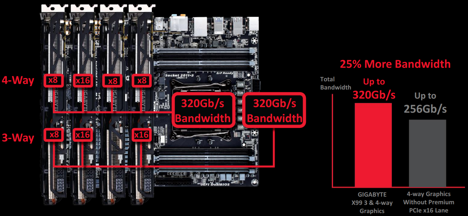
So for example the ASRock motherboard in this review supports only x8/x8/x8/x8, whereas the GIGABYTE X99-UD7 will support x8/x8/x16/x8. There has been some internal discussion because the extra bandwidth might ultimately not make much extra difference to gaming, although it does provide a marketable feature and may be of use to those performing compute based tasks that have bandwidth constraints.
GIGABYTE has also done something slightly different when it comes to PCIe storage, in particular with M.2. M.2 is becoming one of these difficult to predict standards, as it allows PCIe 2.0 x2, PCIe 2.0 x4, PCIe 3.0 x4 and SATA control. This makes it an issue when determining how it is being used on a motherboard. For X99, GIGABYTE is equipping some of its motherboards with two M.2 slots in a stacked configuration, and using one for M.2 based WiFi solutions:
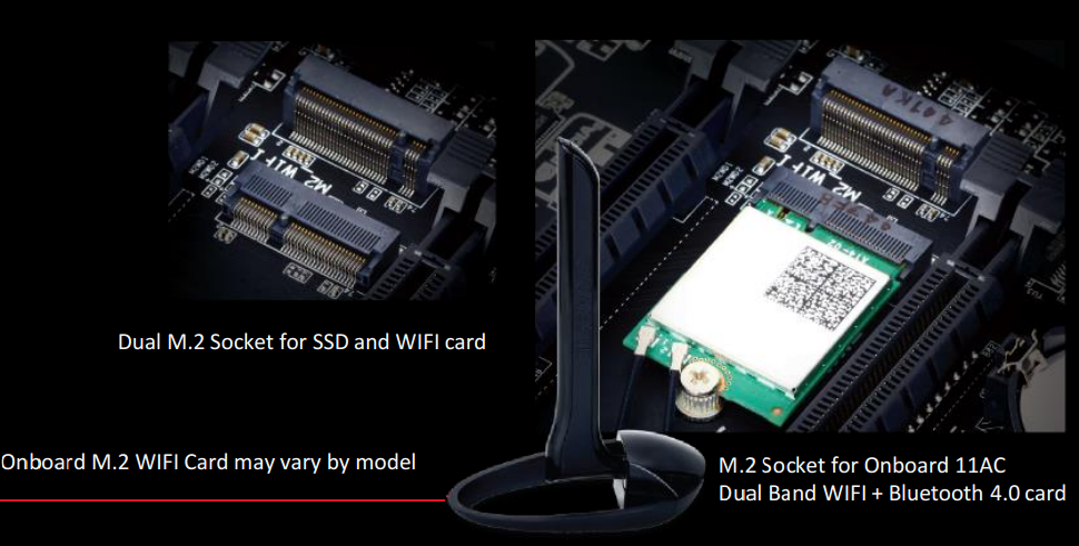
M.2 based WiFi cards have been suggested in the past, although GIGABYTE is going full steam ahead with this implementation, giving connectors to an antenna on the rear panel. This WiFi M.2 slot is at a lower height and has its own screw where needed, with the data based M.2 slot being at a higher height and allowing 2242 to 2280 sized storage devices in a PCIe 2.0 x2 configuration.
For X99 SOC motherboards, GIGABYTE is implementing a ‘Turbo M.2’ socket, with up to 20 Gbps of bandwidth. This means it relies on four PCIe 2.0 lanes from the chipset rather than the CPU, with the thought being that M.2 drives cannot even exploit 20 Gbps at the minute, let alone 32 Gbps. Also, if GIGABYTE did use PCIe 3.0, it would require more configuration alongside the x8/x8/x16/x8 high PCIe bandwidth mode.
GIGABYTE is also introducing a couple of new features for the back panel. One of which we have seen on other motherboards but is new to GIGABYTE – the ability to flash the BIOS without the need for a CPU, DRAM or a GPU to be installed. To go along with the other utilities GIGABYTE provides, this is called Q-Flash Plus.
The feature is actually derived from the Super-IO controller used on board (in this case, an iTE EC 8951E controller), and synchronizes with a single USB port on the rear. With the right named file on the USB stick, it should be a case of plug-in and turn on. An LED will indicate when the process is complete.
The final feature for the rear panel is called ‘Rear Panel LED’, and uses a modified rear panel shield to introduce UV LEDs into the design. When connected with the motherboard, it will cause the back panel to be bathed in a UV glow, making it easier to stick a device in at the dead of night.
Users not too keen on this addition can disconnect the LED and allow the rear panel to go back to normal. The bundled software will allow users to adjust how the rear lights up – either by a constant light, pulsing or responding to the audio coming out of the onboard codec.
GIGABYTE X99-UD7 WiFi Visual Inspection
GIGABYTE announced about ten different SKUs at launch from its Ultra Durable, Gaming and SOC Force lines. With the Ultra Durable units, only certain models will be sold in certain regions. This is going to be true for this X99-UD7, which is aimed more at EMEA (Europe, Middle East, Africa) and APAC (Asia Pacific) than North America which will get the X99-UD5 WiFi instead. The UD5 will be almost identical to the UD7 in feature set, but will have slightly smaller heatsinks and a slightly different bundle, but the underlying design will be the same for both.
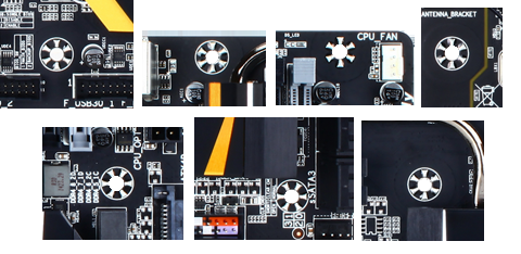
In our UD7 WiFi sample, the heatsinks are all connected via heatpipes with a particularly large chipset heatsink to offset a perhaps smaller one for the power delivery. I had no issue installing any graphics cards or cables due to this arrangement, although the positioning of the heatsinks around the socket does limit where GIGABYTE can put the fan headers. The memory slots alternate between grey and black, with the grey ones to be populated first.
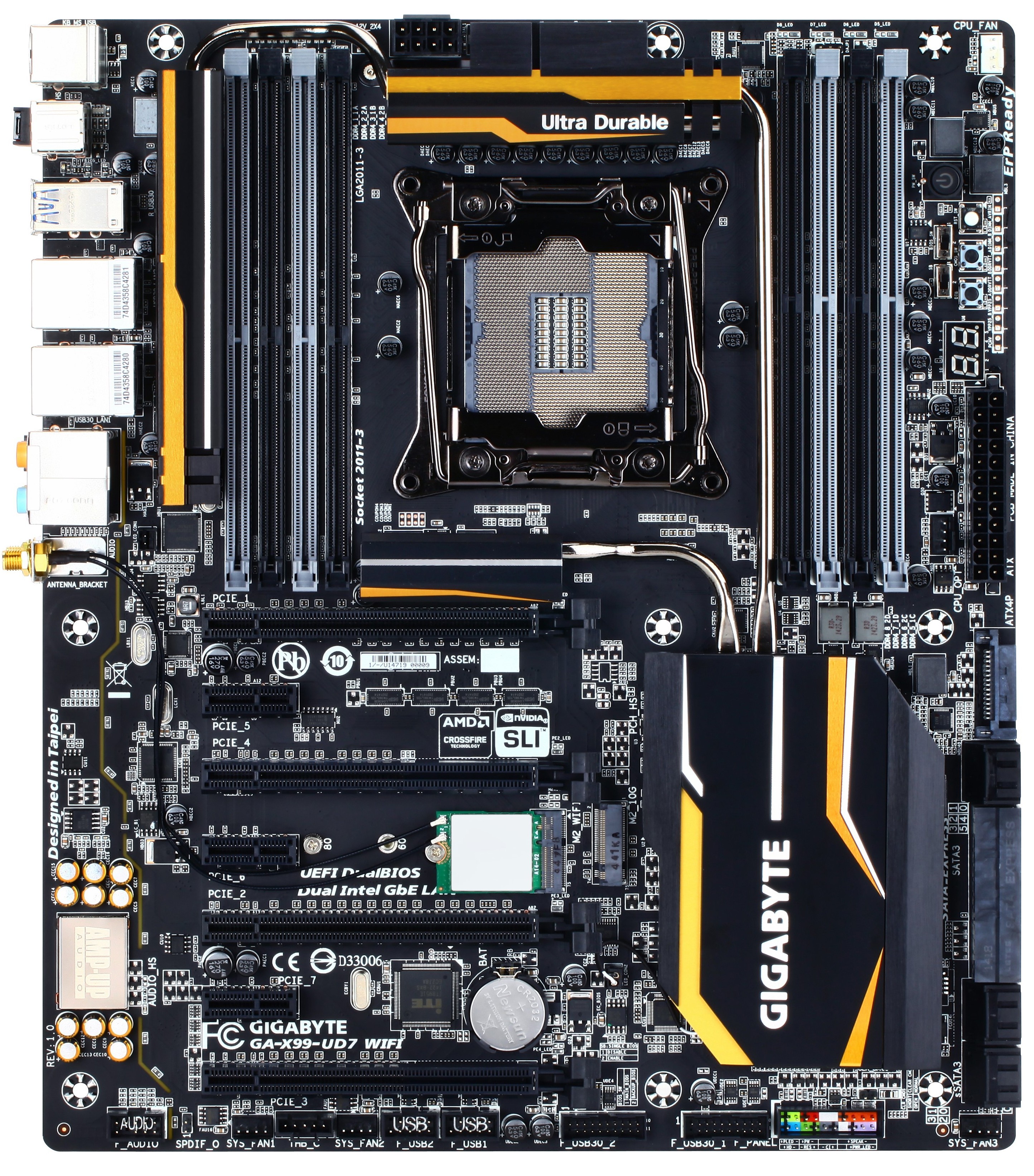
The socket area has only two fan headers within reach due to the heatpipe arrangement – one four pin CPU header in white in the top right of the board, and a 4-pin CPU OPT header next to the 24-pin ATX connector. The other three headers are at the bottom of the board, one on the right and the other two just left of center. These are also 4-pin and labeled as system fans. Having only five fan headers seems relatively few for a high end motherboard.
The power delivery arrangement means that a single CPU 12V 8-pin connector is preset at the top of the board, and most of the extra overclocking options are on the right hand side. Here we get a power button, a reset button, a BIOS switch, a CMOS reset, a switch to enable DualBIOS, and a button to reboot straight into the BIOS.

Underneath these are voltage read points for overclockers, and to the left is a two digit debug display for diagnosing POST problems.
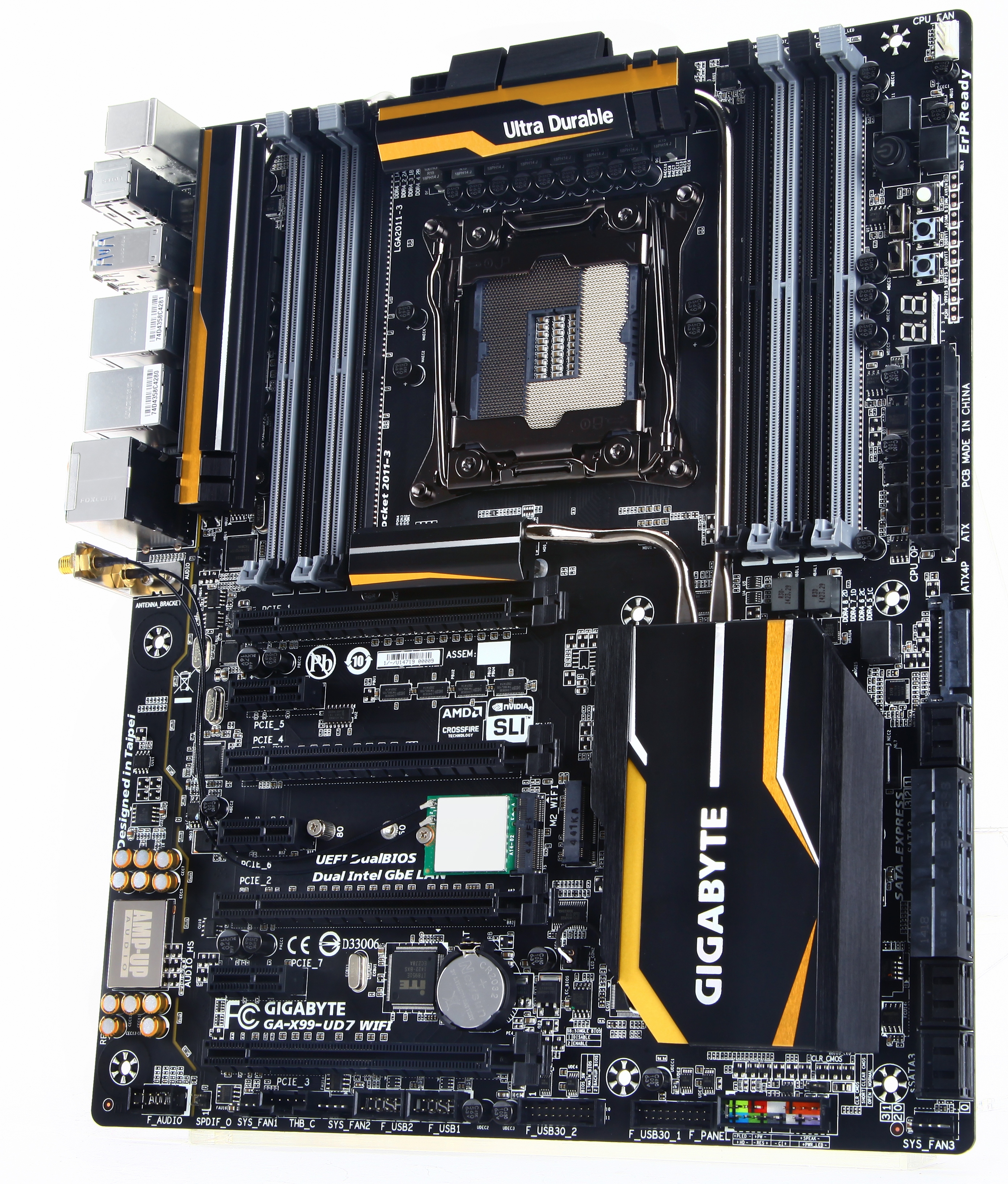
Further down the right hand side is a SATA power connector to add in additional power to the PCIe slots. Out of all the different ways to supply PCIe power, this location is the best: either in the form of a SATA connector or a 6-pin PCIe connector where possible. The 10 SATA ports are split into six RAID capable at the top (listed as SATA) and four more non-RAID at the bottom (listed as sSATA). GIGABYTE is implementing both SATA Express and M.2 on the UD7, meaning that bandwidth is switched between which one is in operation when the machine is turned on.
The bottom of the motherboard features three 4-pin fan headers, a Thunderbolt header, two USB 2.0 headers, two USB 3.0 headers, the front panel audio header and the front panel control header. Both of the USB 3.0 headers are powered by the chipset, with another two from the chipset on the back panel split into eight via dual Renesas USB 3.0 hubs.
For the PCIe arrangement, GIGABYTE has labeled them in a very odd manner. The top port is called PCIe_1, but then follows PCIe_5, PCIe_4 and PCIe_6. PCIe_2 is the third full length slot, with PCIe_7 and PCIe_3 at the bottom.
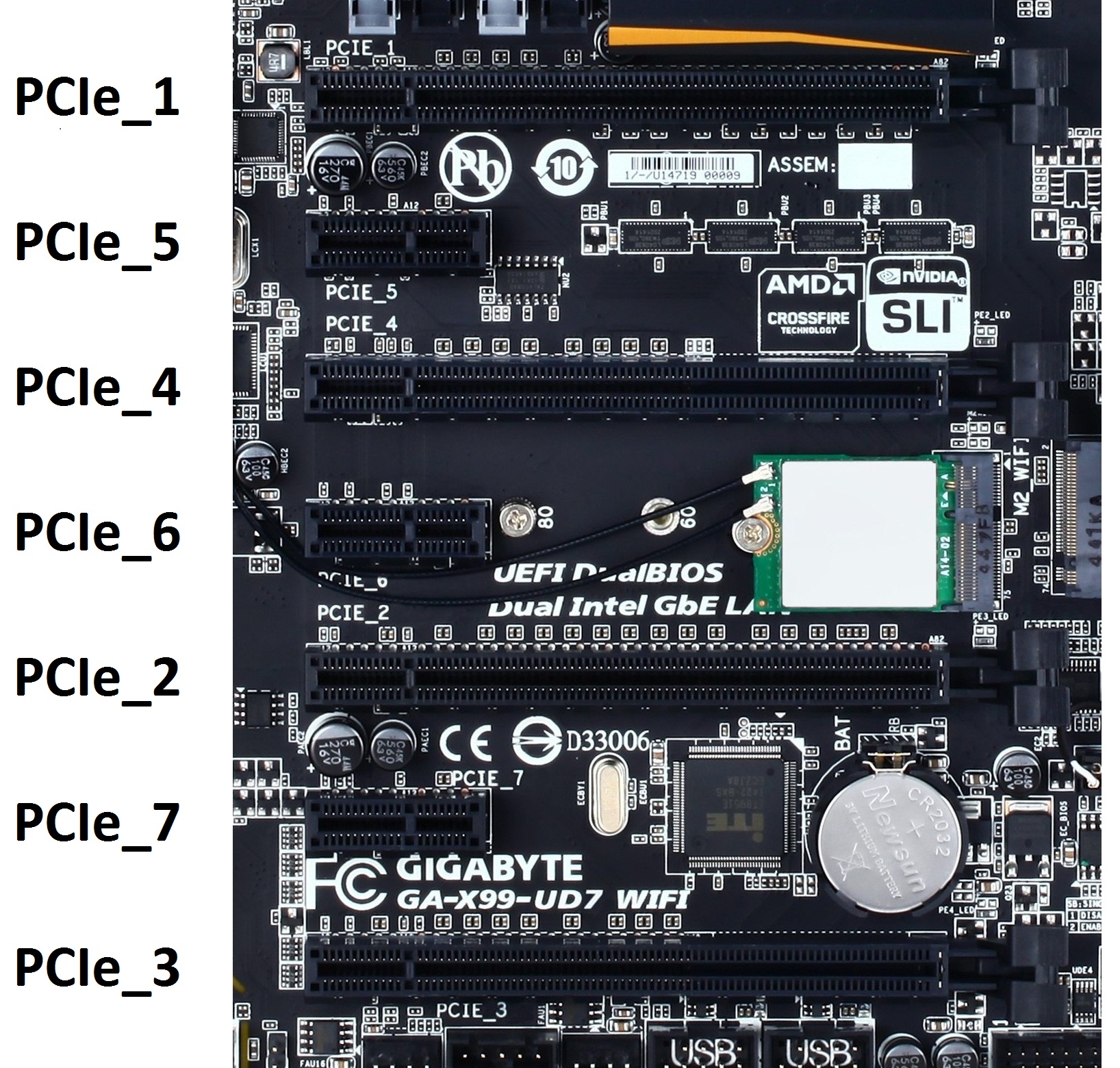
Why this arrangement? So users will fill up the PCIe slots starting with number 1, followed by 2, 3 then 4. This is an odd way of arranging things – a complete contra-strategy to the rest of the motherboard industry who count from the top down. If GIGABYTE plans to make this sort of arrangement permanent, they need a light-up idea like ASUS. If not, then change it back otherwise some users will get headaches.
The following occurs with PCIe 1/4/2/3 full length slots (so from the top of the board down):
CPU with 40 PCIe lanes: x16/-/-/-, x16/-/x16/-, x16/-/x16/x8, x8/x8/x16/x8
CPU with 28 PCIe lanes: x16/-/-/x4, x16/-/x8/x4, x8/x8/x8/x4
Each of these PCIe slots also have the 30-micron gold used by GIGABYTE in its X99 range.
The M.2 arrangement in the middle of the PCIe slots is a little different to the other motherboards in this roundup. Here we have two M.2 slots, but one is being used for the WiFi. The Intel AC7260 was used in our sample, and this uses one PCIe 2.0 lane from the chipset to operate with the antenna reaching around to the rear panel. Our WiFi solution had a plastic tag stuck to the motherboard for the antenna wires to go through, ensuring they stayed close to the PCB and not get in the way of any PCIe devices. The other M.2 slot is a normal PCIe 2.0 x2 solution, capable of either x1 or x2 mode, sharing bandwidth with the SATA Express slot.
The audio next to the PCIe slots is GIGABYTE’s enhanced Realtek ALC1150 audio package dubbed ‘AMP-UP Audio’. Other features such as Op-Amp adjustment and gain switches are not on this model.
The rear of the motherboard, when the shield is used, is fitted with additional UV lighting to add to the aesthetic. There is a 2-pin cable in the shield which fits into a header just behind the two WiFi antenna on the main motherboard PCB.

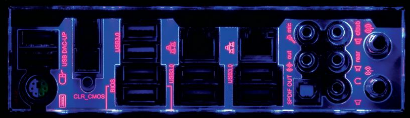
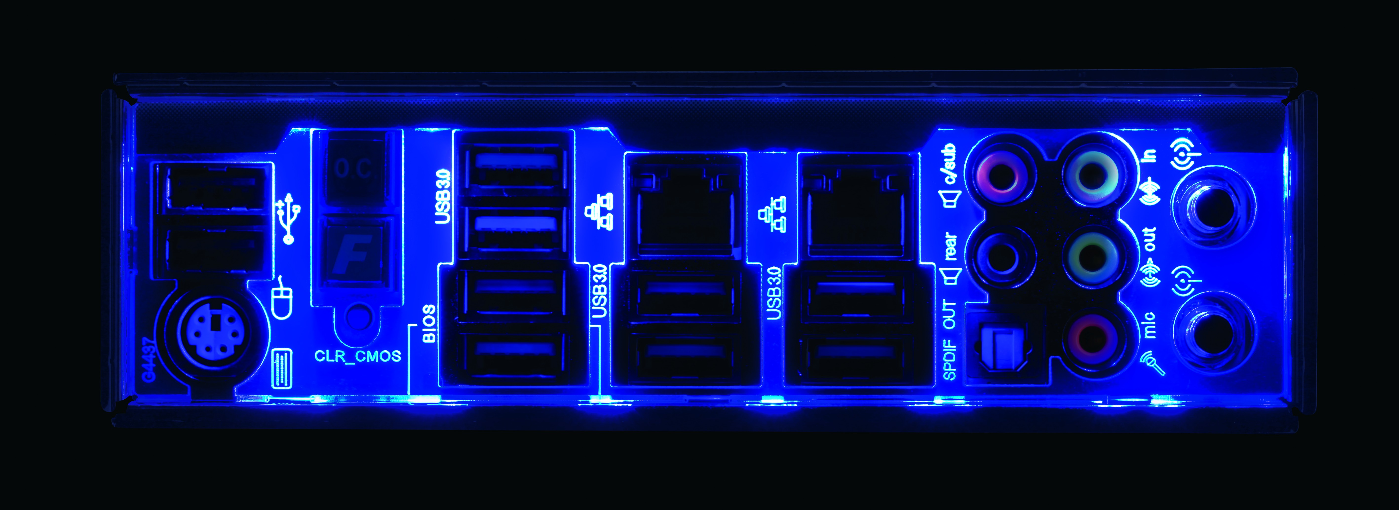
This image is easier to dissect: we get a combination PS/2 port, two USB 2.0 ports, an OC Button, a Fast Boot button, a ClearCMOS button, eight USB 3.0 ports (from Renesas Hubs connected to chipset USB ports), the white Q-Flash port, two Intel network ports (I210-AT and I218-V), audio jacks and dual WiFi antenna.


GIGABYTE X99-UD7 WiFi Board Features
| GIGABYTE X99-UD7 WiFi | |
| Price | US (Newegg) |
| Size | ATX |
| CPU Interface | LGA2011-3 |
| Chipset | Intel X99 |
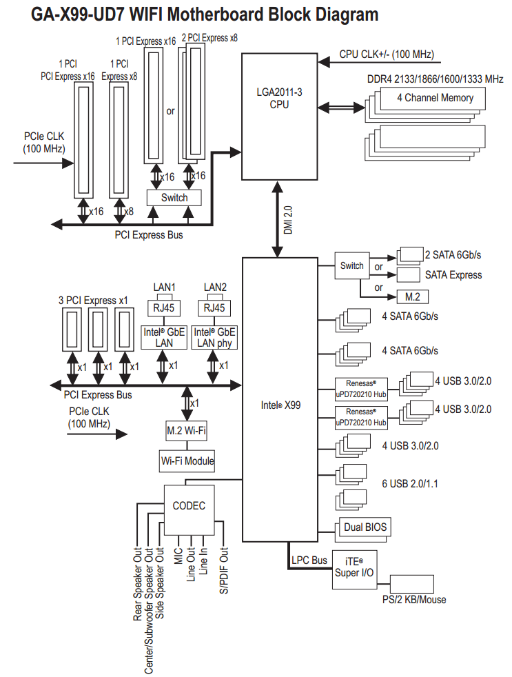
| Memory Slots |
Eight DDR4 DIMM slots supporting up to 64 GB Up to Quad Channel, 2133-3000 MHz Support for RDIMM 1Rx8 Non-ECC |
| Video Outputs | None |
| Network Connectivity |
Intel I210-AT Intel I218-V Intel 7260 AC 2T2R via M.2 |
| Onboard Audio | Realtek ALC1150 via AMP-Up Audio |
| Expansion Slots |
4 x PCIe 3.0 x16 - 40 PCIe: x16, x16/-/x16, x16/-/x16/x8, x8/x8/x16/x8 - 28 PCIe: x16/-/-/x4, x16/-/x8/x4, x8/x8/x8/x4 3 x PCIe 2.0 x1 |
| Onboard Storage |
6 x SATA 6 Gbps, RAID 0/1/5/10 4 x S_SATA 6 Gbps, no RAID 1 x SATA Express 1 x M.2 x2, support for 2242 to 2280 1 x M.2 x1 (WiFi included) |
| USB 3.0 |
4 x USB 3.0 via PCH as two headers 8 x USB 3.0 via Renesas Hubs as eight rear ports |
| Onboard |
10 x SATA 6 Gbps 1 x SATA Express 1 x M.2 x2 5 x Fan Headers 2 x USB 3.0 Headers 2 x USB 2.0 Headers Power/Reset Buttons Two Digit Debug LED Clear CMOS Button Direct to BIOS Button BIOS Switches Voltage Measurement Points Front Panel Header Front Audio Header |
| Power Connectors |
1 x 24-pin ATX 1 x 8-pin CPU 1 x SATA for PCIe |
| Fan Headers |
1 x CPU (4-pin) 1 x CPU-OPT (4-pin) 3 x SYS (4-pin) |
| IO Panel |
1 x Combination PS/2 Port 2 x USB 2.0 Ports 8 x USB 3.0 Ports (via Renesas Hub) - White USB for Q-Flash 2 x Intel Network Ports (I210-AT and I218-V) OC Button Fast Boot Button ClearCMOS Button Audio Jacks 2 x WiFi Antenna Points |
| Warranty Period | 3 Years |
| Product Page | Link |
GIGABYTE is focusing on four-way PCIe orientations across its whole range, whereas most other manufacturers are doing some for three-way and others like this. Five fan headers seems a small amount, but it is interesting to see M.2 used for WiFi in this fashion. I can only assume that GIGABYTE has managed to purchase these in bulk such that the price is similar to a mini-PCIe design – the M.2 design is at least smaller. What GIGABYTE has to consider now is that ASUS is implementing 3T3R, and if a ‘UD9’ type of motherboard at $400 might be worth this sort of adjustment.


62 Comments
View All Comments
gostan - Friday, September 26, 2014 - link
feel like I'm transported back to 2001good job AT!
xunknownx - Saturday, September 27, 2014 - link
what settings on povray is being used in this article? i would love to compare my results against theirs.todo1 - Tuesday, September 30, 2014 - link
X79 supports TRIPLE CHANNEL DDR3, not quad!I don't how it is even possible to make such a mistake?!?
tyaiyama - Wednesday, October 1, 2014 - link
After reading the following:http://www.legitreviews.com/intel-x99-motherboard-...
Is it worth recommendation from Anadtech? Almost 1 month has passed without Asus solving the problem. What's good about this M/B unable to certain hours operations(^^)
tyaiyama - Wednesday, October 1, 2014 - link
BTW, MSI M/B also has an issue.http://www.phoronix.com/scan.php?page=article&...
Both of these M/B happened to be recommended by Anand over the other two: AsRock & Giga. What does it mean? I personally likes AsRock X99 WS which seems Asus X99-E WS w/o PLX.
Haravikk - Thursday, October 2, 2014 - link
Is there a reason the motherboards with moulded shapes over the various I/O ports don't include the I/O shield built-in? I hate adding those damned things; seems unnecessary if your motherboard is shaped around the ports already.Oxford Guy - Saturday, October 4, 2014 - link
Power phases?Also, it seems really lazy to not check what changing the MSI load line calibration setting would actually do if changed. "This is quite odd. It would seem the efficiency of the MSI motherboard when overclocked is somehow stunted..." vdroop is supposed to be part of the Intel specification and load line calibration defeats it, right? So, it looks like there is your answer. Auto isn't the optimal setting.
Also, if you tested these motherboards in the order you reviewed the overclocking results in, you may have fatigued the chip which explains why the results kept getting worse.
woj666 - Monday, October 6, 2014 - link
Agreed, it seems very obvious that that Load Line Calibration setting of "auto" on this MSI board is in fact quite aggressive and applying vboost as described here http://www.anandtech.com/show/2404/5 and here http://linustechtips.com/main/topic/24019-load-lin...The OC section of this article is not comparing apples to apples as the default LLC settings are not the same for the different boards.
akula2 - Tuesday, October 14, 2014 - link
It was a great review, appreciate it very much.1) why Asus X99-E WS is missing out of action?
2) Asus X99-E WS ($510) or Asrock X99 WS ($310)?
My ten X99 ultra Workstations will have the upcoming Maxwell based Nvidia Quadro and Tesla cards? I'm also evaluating Firepro W9100 card too. I don't know if there will be Maxwell based Titan Black (II or whatever name)?
Five builds will have Xeon E5-2680 v3 (more like due to price/performance) or Xeon E5-2690 v3
Five builds will have i7-5760X CPUs
I never used Asrock WS boards earlier, but have many Asus WS boards (X79/Z97). So, what do you think of Asrock WS over Asus X99-E WS in the given configuration above?
Yeah, all Xeon workstations will have Intel P3700 NVMe storage solution. Also, I'm pondering on Synology DiskStation DS2413+ for 48TB NAS solution using WD Red Pro HDDs for those planned ten X99 builds.
Hence, what do you think about those two boards?
3) Did you observe any PCI-e 3.0 limitations/bottleneck on those two boards? Asus X99-E board has 16-four lanes solution? Please clarify on this count.
Thank you
eng.michael - Friday, January 23, 2015 - link
HELLOPLEASE HELP ME
I have one , and i install O.S windows server 2012R2 ,and install all drivers correctly EXCEPT LAN driver , any one can help me in this BIG Problem.
THANKS