MIPS Strikes Back: 64-bit Warrior I6400 Arrives
by Stephen Barrett on September 2, 2014 10:00 AM ESTThe MIPS I6400 CPU
Like the Cortex-A53, the I6400 is an in-order, dual-issue design. Each processor supports IEEE 754-2008 floating point operations, 128-bit SIMD instructions, and hardware virtualization. ARM has previously stated that Cortex-A9 is roughly 2.5 mm2 of area with a 40 nm process, and Cortex-A53 is 40% smaller at the same process, placing it at roughly 1.5 mm2 of area. At 28nm, we can estimate a Cortex-A53 is about 1mm2. Comparatively, MIPS states the I6400 is 1mm2 on the TSMC 28nm HPM process in "worst-case scenarios". Therefore the designs are quite comparable.
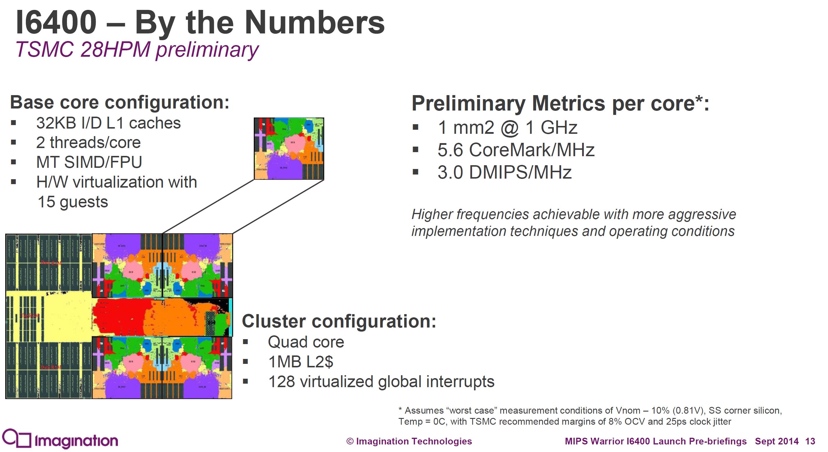
Differences between the Cortex-A53 and I6400 start with a 9 stage pipeline in the I6400 vs 8 stages with the A53, theoretically allowing the I6400 to clock higher. However the I6400 is 9 stages for all operations, whereas the A53 is 8 stages for integer but 10 for NEON/Floating Point operations.
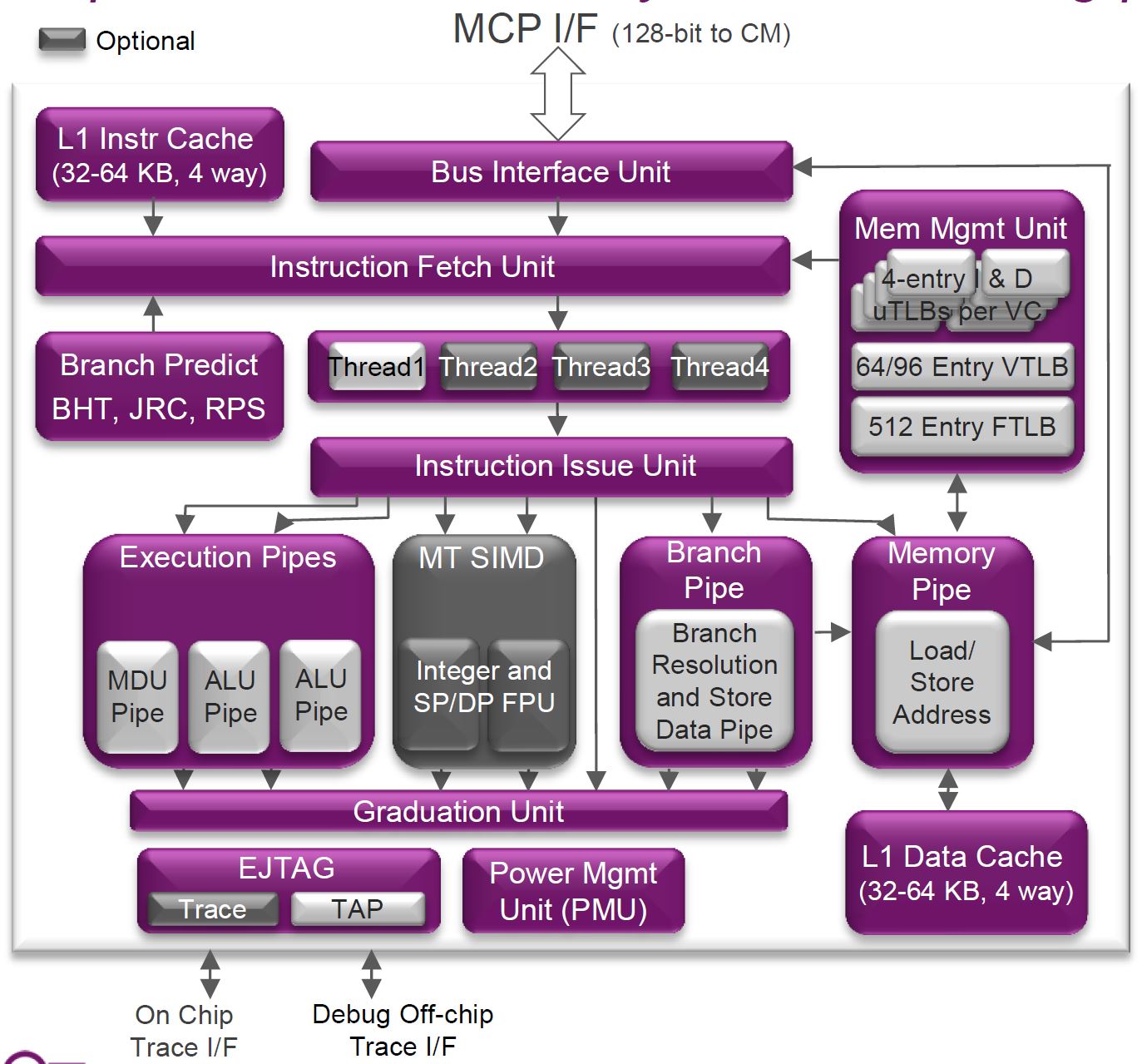
If you look closely at the block diagram you can see one of the I6400’s interesting tricks: Simultaneous Multi-Threading (SMT). Avid readers of AnandTech should recognize this technology immediately. It has been utilized by Intel since the venerable Pentium 4, over a decade ago in 2002, under the trademarked name Hyper-Threading. While the Core Duo and Core 2 lines dropped support for Hyper-Threading, the Nehalem (Core i7) and later processors have continued its use. IBM's POWER cores also support SMT (up to 4-way SMT with POWER7 and 8-way SMT with POWER8).
Strangely, we have not seen anyone else (e.g. ARM or AMD) implement this same technology until now. AMD has a partial implementation in its Bulldozer architecture, with each "module" in their current CPUs/APUs providing two full integer cores with some shared elements. AMD contends that their partial SMT implementation is actually better for some workloads, but that's a different discussion. Regardless, SMT support it is new to the small-core space.
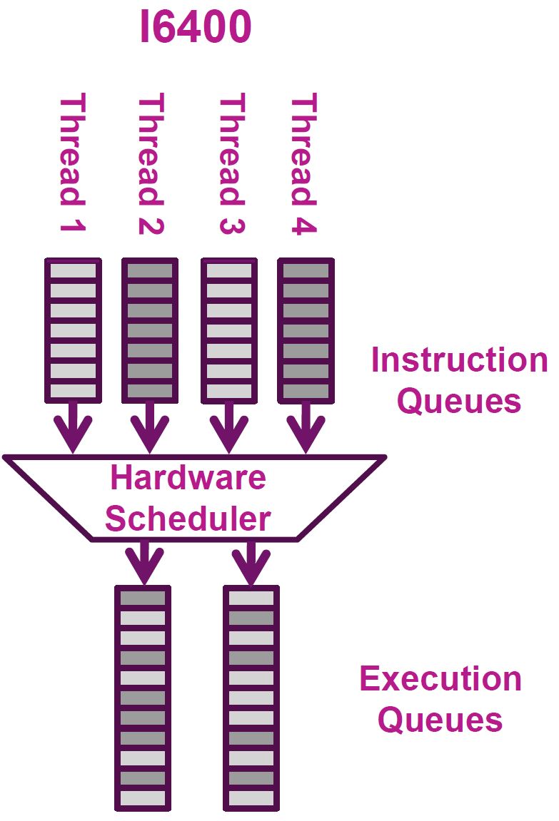
An SoC designer licensing an I6400 core can decide how many threads of SMT they want to implement into the core, from 1 to 4. The physical core then advertises itself to the operating system as 1 to 4 logical cores, thus allowing the OS to send up to four threads of instructions to execute at any given time. The hardware’s execution scheduler can then, per cycle, dynamically switch between threads depending on which hardware resources are available. For example, if the integer ALUs are tied up with threads 1-3 but thread 4 only needs floating point resources, the scheduler can schedule thread 4 to the FP units instead of waiting around.
Imagination claims their MIPS core featuring SMT only increases 10% in size but increases an incredible 30% to 50% in performance. A 3x to 5x size to performance ratio for any given feature is quite hard to come by. If Imagination’s claims are correct, it’s a wonder this feature is optional. Certain applications greatly suffer from SMT, namely real-time applications that depend on determinism, but like Intel Hyper-Threading, I would hope there is a simple software setting to disable this feature when it is not desired. Imagination specifically calls out networking applications (which are very throughput focused) as greatly benefiting from SMT, which is the optional MIPS MT extension.
Even though the core is in-order, the I6400 performs superscalar execution for a given thread. Since it is dual dispatch, two instructions from a single thread can be executed in parallel. I would imagine the superscalar execution is limited to the next two instructions within a thread (as there is no reorder buffer); otherwise the entire core wouldn’t be listed as in-order.
| Mid-Class CPU Core Comparison | ||||||
| MIPS I6400 | ARM Cortex-A53 | |||||
| CPU Codename | Warrior | Apollo | ||||
| ISA | MIPS3264 Release 6 | ARMv8-A (32/64-bit) | ||||
| Cores in an SMP Cluster | 1-6 | 1-4 | ||||
| Thread Width | 1-4 | 1 | ||||
| Issue Width | 2 micro-ops | 2 micro-ops | ||||
| Reorder Buffer Size | None: In-Order | None: In-Order | ||||
| Pipeline Depth (stages) | 9 | 8 (Int) 10 (FP) | ||||
| Integer ALUs | 2 | 2 | ||||
| Load/Store Units | 1 (2 with bonding) | 1 | ||||
| Load Latency | 3 cycles | 3 cycles | ||||
| Branch Units | 1 | 1 | ||||
| FP/NEON ALUs | 2 | 2 | ||||
| Coherency | Directory | Snoop + Filter | ||||
| L1 Cache | 32 or 64KB I$ + 32 or 64KB D$ | 8 to 64KB I$ + 8 to 64KB D$ | ||||
| L2 Cache | 0.5 to 8MB | 0.5 to 2MB | ||||
Another trick the I6400 employs is called instruction bonding or load/store bonding, which probably ties in with the previously mentioned hardware scheduler. If two load or store instructions arrive at the scheduler with adjacent addresses, the I6400 can "bond" them together into a single instruction executed by the load/store unit. Two 32-bit integer accesses will be bonded into a single 64-bit integer access, two 64-bit integer accesses bond into a single 128-bit integer access, and two 64-bit floating point accesses bond into a single 128-bit FP access.
Applications often perform memcopies that move relatively large amounts of memory from point A to point B, resulting in a long list of load/store instructions. This hardware scheduler feature can halve the time required to fulfill a memcopy request and is completely transparent to software. MIPS states this feature is a natural expansion of their load/store unit, as their bus widths are already 128-bits to support their SIMD unit. Doubling the efficiency of the I6400's single load/store unit (in certain cases) helps save area and power compared to duplicating the unit entirely.
Directory Based Coherency
One of the largest problems a multicore processor needs to solve is coherency. Multiple PhDs have been earned on this topic alone. The core of the problem (pun intended) is that multiple execution resources (CPU or GPU cores) exist each with their own L1 data cache. If Core1 writes to address 0xABC0FF, its L1 data cache is immediately updated. However, what if there is another core present that also has the data at address 0xABC0FF cached? Its cached data is now invalid and, if used, results in computational inconsistency and a potentially critical application errors.
There are multiple techniques to deal with this problem. The most common is called snooping. Each core in a multicore system monitors the L1 cache lines of every other core. If a write is observed to an address that is locally cached, that cache line is immediately invalidated. When an invalidated cache line is accessed, the invalid data is not returned but rather a longer trip out to the coherent L2 cache is made. Since all the L1 caches update whenever any L1 cache is written to, this is the most performant coherency implementation. However, it is quite complex. If eight cores are designed with coherent L1 caches, each core must connect to seven other cores, causing an explosion of complexity.
One way modern designs deal with increasing snoop complexity is by using a "snoop bus". Instead of connecting all cores L1 caches to each other, all cores are connected all to a shared bus. When a core writes to an L1 cache location, it broadcasts the address written to all other cores on the snoop bus. Other cores then invalidate that address if it is present in their L1 cache. This helps with wiring inside the chip, but snoop traffic is still increasing with added cores. ARM's A53 goes a step further and has a Snoop Control Unit (SCU) that sits on the bus and filters out snoop traffic based upon which caches have which addresses.
The I6400 uses the other common technique, directory based coherency. The L2 cache in the I6400 maintains a listing of all the data being duplicated in attached CPU cores. When an address is changed, the directory is always notified. The directory can then update the attached CPU cores that have duplicated that data. In the worst-case scenario this is both higher latency (informing the directory of a write takes time) and can result in increased bus traffic because every core could have cached a particular address. However, it’s not likely that every single core would have cached the same data that gets overwritten. Either way, it is significantly simpler to implement as it is a single point to point connection between L1 and L2 per core rather than a web of connections between L1s. This is likely a contributing factor in why the I6400 can be used in SMP clusters of 6, whereas the A53 is limited to SMP clusters of 4.

Finally, the I6400 includes fine grained power consumption optimizations branded as “PowerGearing” by MIPS. The processor can disable clocks (clock gating) to individual CPU cores, caches, and subsystems (such as SIMD blocks). Each CPU core can individually sleep and be controlled by OS Dynamic Voltage and Frequency Scaling (DVFS), which is essential to Android/Linux processor power management.


84 Comments
View All Comments
Exophase - Wednesday, September 3, 2014 - link
Hi Alex, could you clarify what you mean by this comment? Superscalar and in-order are completely orthogonal properties, and I would expect that it always behaves like an in-order design regardless of SMT. Do you mean that in SMT mode it can only dispatch one instruction per cycle from the same thread? If that's the case, surely this is something that can be dynamically configured based on active thread count and not a fixed property of the processor?MartinT - Thursday, September 4, 2014 - link
I guess it is true strictly speaking that because of the two execution queues, it's limited to either super-scalar (single-threaded) or (scalar) multi-threaded operation at any one instant.I agree that it should read 'scalar' rather than 'in-order'.
mthrondson - Sunday, September 7, 2014 - link
To clarify - the I6400 can run superscalar on a single thread, or issue from two threads simultaneously. And it can switch which thread(s) it is working from on a per cycle basis.Guspaz - Tuesday, September 2, 2014 - link
They taught us MIPS32 assembly in school. My impression was that it was enormously simpler to write by hand than x86 assembly, much less of a headache to work with. Of course, assembly is almost entirely irrelevant these days.patrickjchase - Tuesday, September 2, 2014 - link
The main reason everybody learns MIPS (a.k.a. "DLX") in school is because the dominant architecture text was co-written by MIPS' inventor.Guspaz - Tuesday, September 2, 2014 - link
That's entirely possible. To be honest, I don't remember which textbook we used for our processor architecture course. But it was a breath of fresh air compared to x86 or even SIC. Having all the registers be general-purpose and letting you specify which register to put results into in the instruction was much easier to work with when writing assembly by hand on paper than x86, where every register seemed to be special-purpose, with different instructions putting results in different abstractly named registers.Exophase - Wednesday, September 3, 2014 - link
I've written x86 and MIPS assembly in real world applications, and personally I find both to be pretty annoying. When writing MIPS assembly, the poor addressing modes, delay slots, and range of immediates make it more cumbersome than x86. When writing x86 assembly, the lack of registers and three-address operands make it more cumbersome than MIPS. I haven't written much in x86-64, which I suspect is less annoying.dwforbes - Tuesday, September 2, 2014 - link
It's worth noting that for Android developers using the NDK, coding for MIPS, ARM64, or x86-64, is in the vast majority of cases nothing more than a compiler flag. There is seldom extra work necessary unless you've specifically used inline assembly.Samastrike - Tuesday, September 2, 2014 - link
I couldn't help noticing that the android logo used in the slide on the second page is holding a lollipop. Is this some confirmation of the official name when android L releases?Stephen Barrett - Tuesday, September 2, 2014 - link
I had the same thought. Wondered if someone would notice that. I'll let everyone conjecture on that topic :)