Intel Broadwell Architecture Preview: A Glimpse into Core M
by Ryan Smith on August 11, 2014 12:01 PM ESTPutting It All Together: Low Power Core M
So far we’ve discussed Broadwell’s architecture on a broad basis, focusing on features and optimizations that are fundamental to the architecture. However to talk about the Broadwell architecture is not enough to fully explain the Core M itself. Though many of Core M’s improvements do come from Broadwell, Intel has also made a number of alterations to everything from the CPU packaging to the process node itself specifically for Core M. It’s the resulting combination of these factors that has allowed Intel to iterate on Broadwell-Y over Haswell-Y, and why Intel is so confident in Broadwell-Y’s capabilities and suitability for mobile form factors.
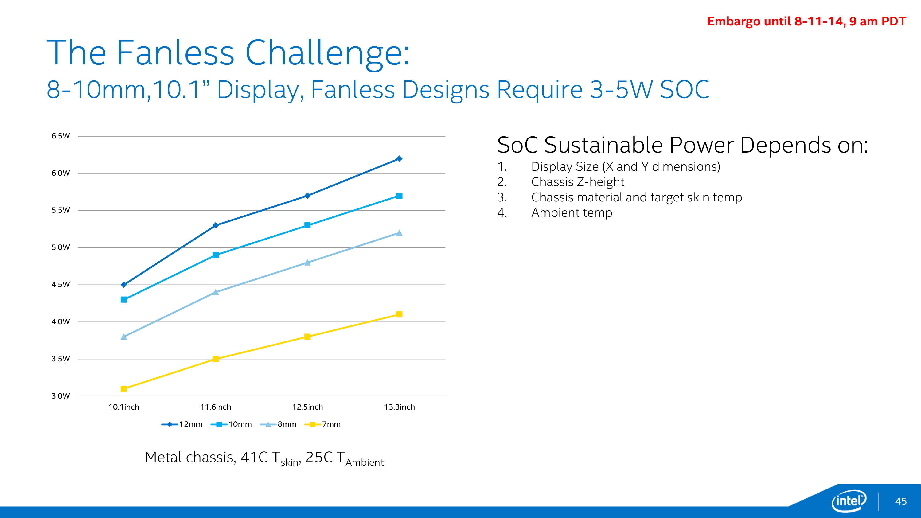
When it comes to building and configuring Core M, Intel likes to refer to their efforts as the “Fanless Challenge,” reflecting the fact that their biggest goal with Core M is to comfortably get the processor in to 10” tablets under 10mm in thickness that are passively cooled. A big part of getting into such a device is meeting the heat dissipation limitations of the form factor – a 10” tablet under 10mm would require a sub-5W SoC – which is where a lot of Intel’s engineering efforts have gone. Broadwell’s performance optimizations, the GPU optimizations, GPU duty cycling, and the 14nm process all contribute to getting a Core CPU’s power consumption down to that level.
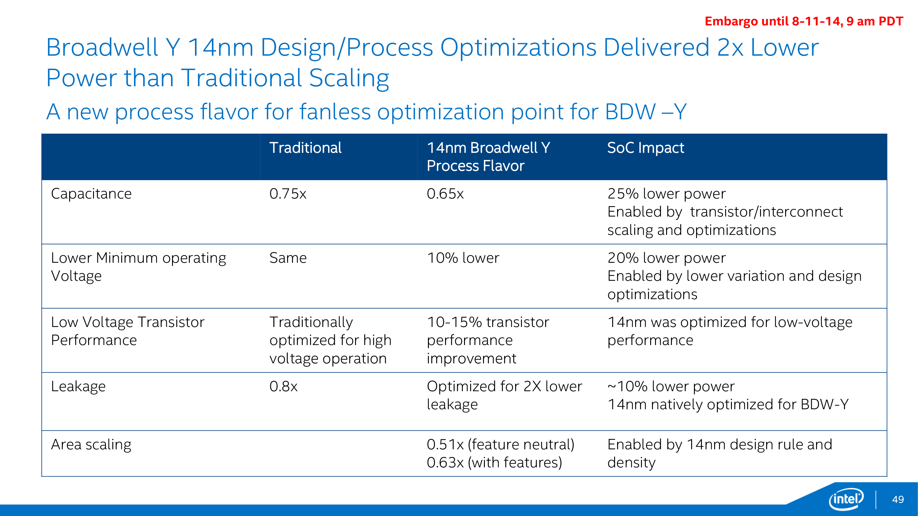
But even that’s still not enough, and for Core M Intel went so far as to give Broadwell-Y its own die and design a low-power optimized version of their 14nm process just for it. This variant is designed to further reduce power consumption by optimizing the resulting transistors for lower power, lower voltage, lower clockspeed operation. By doing this Intel was able to further reduce power consumption in all of the major areas over what would be a traditional 14nm Intel process.
In the resulting 14nm Broadwell-Y process, voltage, capacitance, and leakage were all improved over the traditional 14nm process. Capacitance was reduced by 15%, minimum operating voltages by 10%, and leakage was improved to the point that it reduced SoC power consumption by 10%. The combination of all of these factors serves to significantly lower power consumption over what Intel’s traditional 14nm process would provide.
Working in concert with Broadwell-Y’s 14nm process, Intel has made a number of other changes to further reduce power consumption. Some of these are reflected in Broadwell’s overall design and others are unique to Broadwell-Y, such as using a lower TjMax for Broadwell-Y. By reducing the maximum operating temperature of the chip Intel has been able to realize further power savings by further reducing voltage and decreasing the maximum amount of temperature-dependent leakage the SoC will experience.
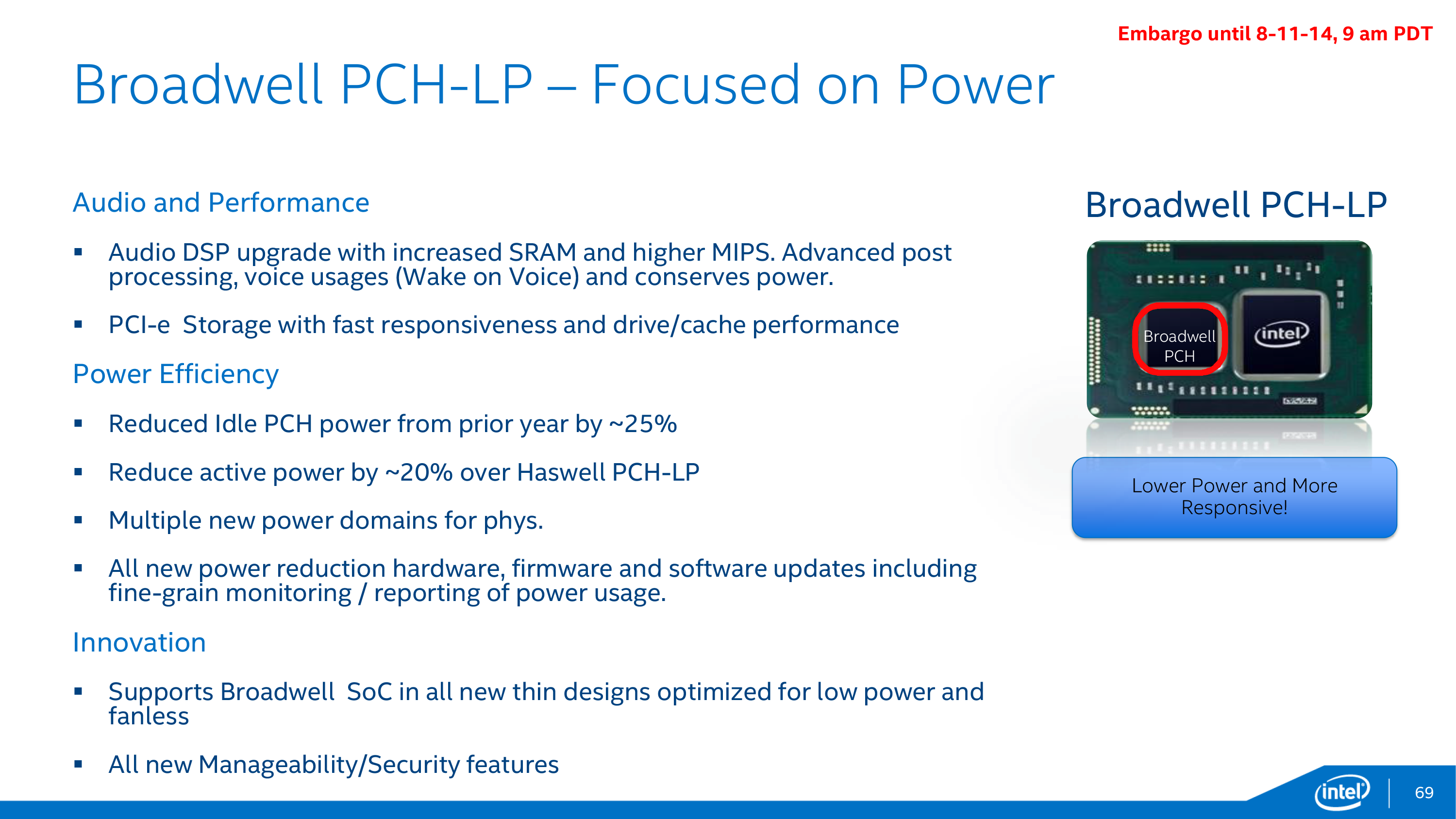
Meanwhile Broadwell-Y’s partner in crime, the on-package PCH, has received its own optimizations to reduce power consumption on the SoC’s total power consumption. The PCH itself is not much of a power hog in the first place – it’s still made on Intel’s 32nm process for this and cost reasons – but with such a strong focus on power consumption every watt ends up counting. As a result the Broadwell PCH-LP has seen optimizations that cut its idle power consumption by 25% and its active power consumption by 20%. Further improvements to the PCH’s monitoring hardware also mean it’s more responsive and can be controlled to a finer degree than the Haswell PCH-LP, and Intel has upgraded to a faster audio DSP to improve performance and reduce power consumption there as well.
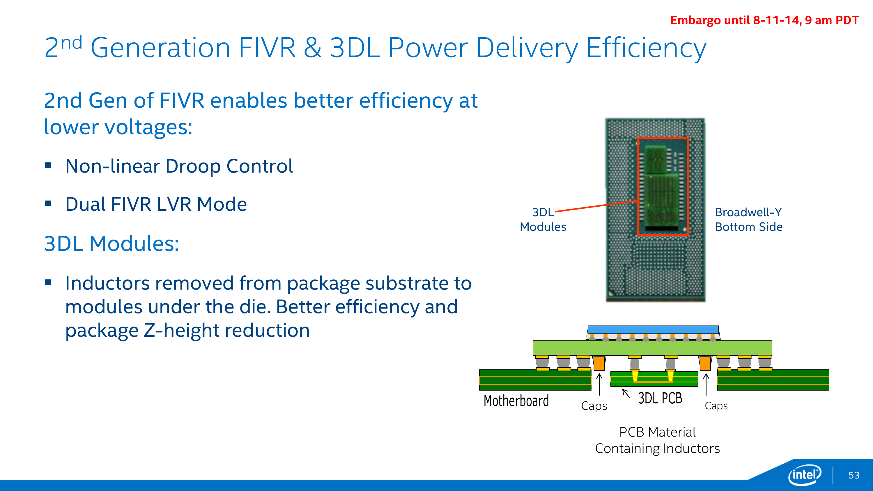
Feeding all of that silicon in turn is Intel’s second generation Fully Integrated Voltage Regulator (FIVR), which further builds off of Intel’s other optimizations. The 2nd gen FIVR has been tuned for Broadwell-Y’s lower voltages, making the FIVR itself more efficient when delivering power at those voltages. To accomplish this Intel has implemented non-linear vDroop control, which is designed to better control the voltage when workload changes would cause voltage overshoots that waste power. And when even the 2nd gen FIVR isn’t efficient enough, this latest FIVR offers a second mode (LVR Mode) for low voltage/workload situations where the FIVR can be partially bypassed to reduce the FIVR’s power consumption.
Interestingly Broadwell-Y also sees the voltage regulation inductors redesigned and relocated in both the name of power efficiency and space efficiency. We’ll get to the case of space efficiency in a moment, but for power efficiency the new 3D inductors (3DLs) have been placed on the underside of the package, allowing the use of more efficient inductors that waste less power.
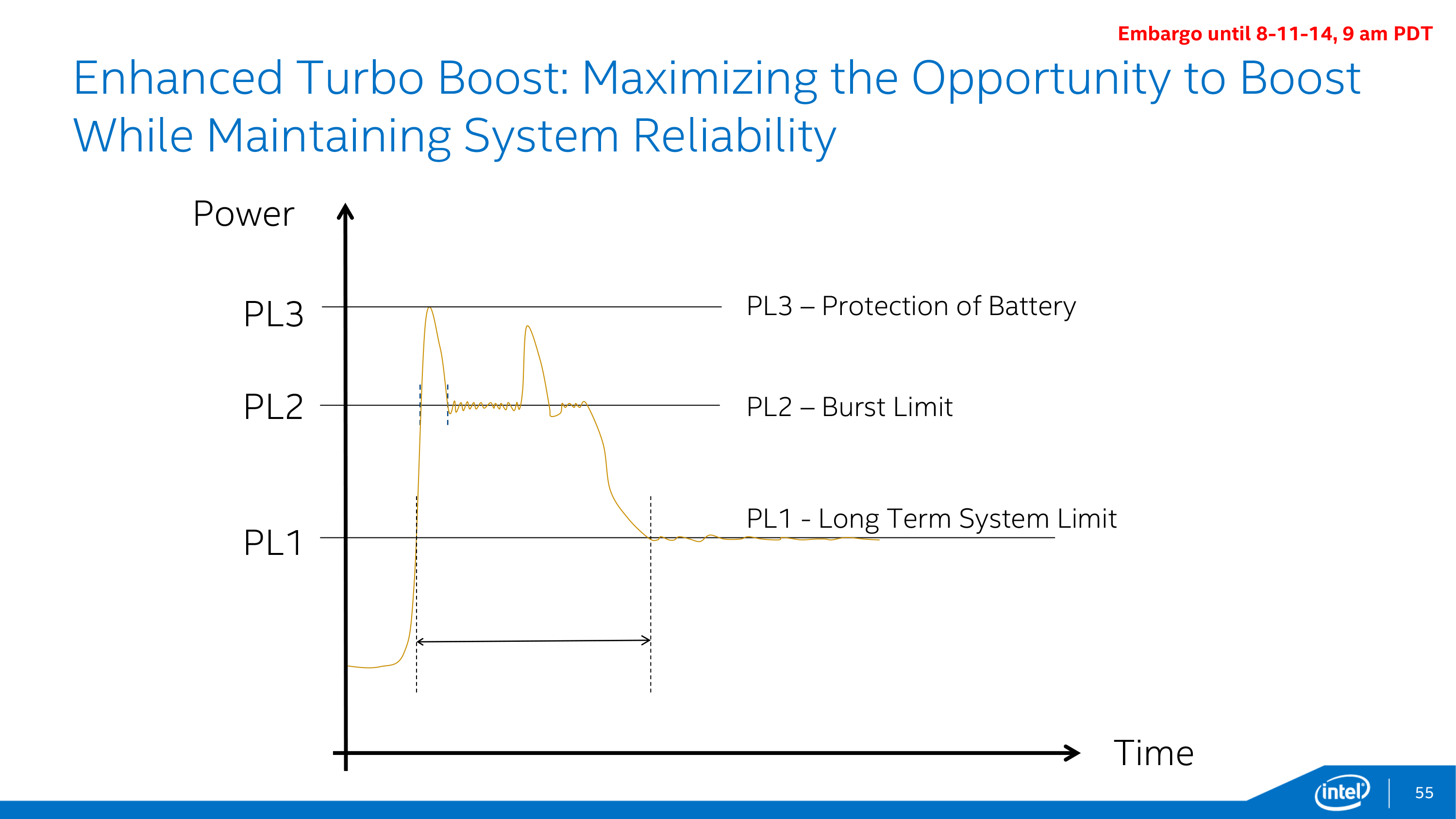
This brings us to the final element of Intel’s power optimization efforts, which involve further adjustments to turbo boost as part of Intel’s “hurry up and go to sleep” motto. New for Broadwell-Y is a 3rd power state, PL3, which allows for even greater turbo boosting, but for only a very limited period of time – on the order of milliseconds. PL3 represents the maximum amount of power the device battery can deliver, and while it’s okay to reach this value sparingly, PL3 is a fast drain that is very hard on the battery. The existence of PL3 in this case is as much for battery protection as it is for performance; it allows devices to tap into PL3 power levels on occasion, all the while allowing PL2 (the regular burst limit) to be defined at a safer value below the battery’s limit. Put another way, by knowing PL3 devices know how to stay farther away from it, which in the long run is what’s best for battery reliability.


158 Comments
View All Comments
Hrel - Tuesday, August 12, 2014 - link
". Intel has made it clear that they don’t regress on clockspeeds"lol, they often regress on clockspeeds.
nikolayo - Wednesday, August 13, 2014 - link
This sounds as a distraction meant to divert attention from the fact that Intel is about a year late with 14nm. It seems than the Moore's law will stop working quite soon. I would still bet on Intel being able to implement 10nm but that will likely be the end of the road for the current technology. And there is no clearly visible path beyond that. Not that progress will stop but it may slow down to the pace we observe e.g. in car design and production rather than what we are used to expect in chip design and production.asoltesz - Wednesday, August 20, 2014 - link
Car design and production is being turned upside down by electric cars like Tesla.Apart from the comparisson, you may be right.
lagittaja - Wednesday, August 13, 2014 - link
Honestly. After reading the article. Which was really a good read and huge thanks to Ryan. All I can say is. Amazing. That is all.Oxford Guy - Thursday, August 14, 2014 - link
"Intel’s solution to this problem is both a bit brute force and a bit genius, and is definitely unlike anything else we’ve seen on PC GPUs thus far. Since Intel can’t reduce their idle voltage they are going to start outright turning off the GPU instead;"That qualifies as genius these days? The most obvious method to reduce a GPU's power consumption is to turn it off.
c plus plus - Saturday, August 16, 2014 - link
intel is really amazing and i hope broadwell doubles both gpu and cpu performance with the help of magicMr Pras - Tuesday, August 19, 2014 - link
I liked the comments in this thread but was disturbed by the fan boys. Just because there was an amd marketer here doesn't mean that we should resort to intel worship. At least for me, those discussions are totally moot in this thread.Blaiser - Wednesday, September 17, 2014 - link
Can somebody clarify this for me?Broadwell Core M is supposed to support fanless designs. Will Broadwell-U support fanless as well? Meaning will high end laptops with Broadwell-U be fanless? If not, will Skylake be able to have high end machines be fanless?