ARM’s Mali Midgard Architecture Explored
by Ryan Smith on July 3, 2014 11:00 AM ESTMidgard: The Modern Mali
As ARM’s current-generation SoC GPU architecture, at the highest level the Midgard architecture is an interesting take on GPUs that in some ways looks a lot like other GPUs we’ve seen before, and in other ways (owing to its uncommon ancestry) is radically unlike other GPUs. This is coupled with the fact that as an SoC GPU supplier, ARM is in an interesting position where they can offer both CPU and GPU designs to 3rd party licensees, unlike most other GPU designers who either use their designs internally (Qualcomm, NVIDIA) or only license out GPUs and not ARM CPUs (Imagination). From a sales perspective this means ARM can offer the CPU and GPU designs together in a bundle, but perhaps more importantly it means they have the capability design the two in concert with each other, being in the position of the sole creator of the ARM ISA.
Architecturally Midgard is a direct descendant of Utgard. While there is a significant difference in how unified and discrete shaders operate, and as a result they cannot simply be swapped, the resulting shader design for Midgard still ends inheriting many of Utgard’s design elements, features, and quirks. At the same time the surrounding functionality blocks that compose the rest of the GPU have received their own upgrades over the years to improve performance and features, but are none the less distinctly descended from Utgard as well. At the end of the day this is a distinction more important for programmers than it is users (or even tech enthusiasts), but going forward it’s interesting to note just how similar Utgard and Midgard are, a similarity we don’t normally see between unified and discrete shader designs.

From a design standpoint Midgard is designed to span much of the range for SoC GPUs, from cheap, area-efficient designs to relatively massive designs with an eye on gaming. In doing so ARM offers a few different variations on the Midgard design that are all architecturally identical, but will vary slightly in features and internal organization. So for the purposes of today’s article we’ll be focusing on ARM’s latest and greatest design, Mali-T760, but we will also be calling out differences as necessary.
First and foremost then, let’s talk about design goals and features. Unlike the bare bones OpenGL ES 2.0 Utgard architecture, Midgard has been designed to be a more feature-rich architecture that not only offers solid graphics performance but solid compute performance too. This is in part a logical extension of what a unified shader GPU can already do – they’re innately good at mass math for graphics, so compute is only a minor stretch – but also a deliberate decision by ARM to push compute harder than they would otherwise have to for merely a graphics product.
From an API standpoint then Midgard was designed as what is best described as an OpenGL ES 3.0+ part. The architecture was designed from the start to offer functionality beyond what OpenGL ES 3.0 would offer, a decision that has since benefitted ARM by allowing Midgard parts to keep up with newer API standards. In fact ARM has just recently completed OpenGL ES 3.1 conformance testing, with their updated drivers passing Khronos’s required tests. As such all Midgard parts at a hardware level can support OpenGL ES 3.1, with software support reliant on OS and device vendors shipping updated OSes and drivers that enable 3.1 functionality.
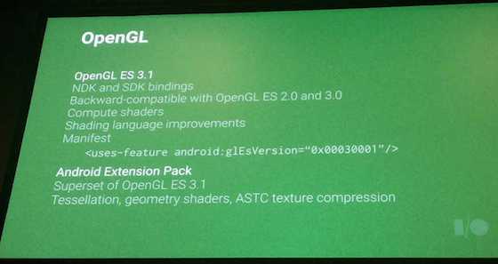
Even then Midgard has some functionality that has gone untapped, but will be enabled in the Android ecosystem through the upcoming Android Extension Pack for Android L. The AEP will further build off of OpenGL ES 3.1 by enabling features such as tessellation and geometry shaders, features that did not make it in to 3.1. As with OpenGL ES 3.1, ARM has confirmed that they expect all Midgard GPUs to support the AEP.
Finally, along with OpenGL ES support, ARM also officially offers Direct3D support on Midgard. This functionality has not yet been tapped – all Windows Phone and Windows RT devices so far have been Qualcomm or NVIDIA based – but in principle it is there. One thing to note however is that among the Mali 700 series, only Mali-T760 is Direct3D Feature Level 11_1 capable. Mali-T720 however only supports level 9_3, more befitting of the market realities and its status as a lower cost, lower complexity part.
Meanwhile from a compute standpoint Midgard is intended to be a strong competitor by supporting Android’s RenderScript framework and OpenCL 1.2 full profile. OpenCL support on SoC GPUs has been spotty due in part to the fact that the major OSes haven’t consistently supported it (iOS never has and Android only recently), and of those SoC GPUs that do support it, not all of them support the full profile as opposed to the much more restricted embedded profile. As is often the case with GPU computing just how well this functionality is used is up to the capabilities and imaginations of developers, but ARM has made it clear that they’re fully backing GPU computing even in the SoC space.


66 Comments
View All Comments
seanlumly - Thursday, July 3, 2014 - link
Given the "exotic" the ILP and the 128-bit VLIW SIMD, the Mali looks like an impressive performer. If a Mali T760MP10 is indeed a part fit for smartphone-level power consumption, then a quick linear-scaling -- given GFXBench scores of a T760MP4 -- would imply that such a GPU is very competitive with something like the adreno 420 and certainly impressive if scaled up further to a tablet-level power consumption. If, however, an MP10 consumes roughly as much as a K1 or GX6650, then I'm very sceptical about its competitive performance.I find the distribution of ALUs to memory units strange given mobile bandwidth limits. The Mali T760 in an 8-core configuration clocked at 600MHz will allow for 19.2 GB/s of load/store access (256-bits/clock: source ARM). This is quite high memory bandwidth, and an increase in GPU clocks or cores will likely yield idling load/stores units doing nothing but taking up valuable die area. Operations with high varying access, cache reads, and tile read/writes will of course make good use of these additional units, but it still seems like overkill on all but very memory-access heavy apps. ARM would know best, though I'm suspicious that so many load/store units are needed for common workloads. I would guess that in common scenarios, bandwidth to main memory would be exhausted long before all of the memory units were fully utilized on a Mali T760 of high core count (eg. MP12-16).
Decoupling the load/stores and texture units as their own "core" may allow more appropriate scaling to fit the bandwidth of the target system. A system with an ultra-high resolution, could be endowed with more load/stores and/or texture units. A system with a lower resolution could use less and opt for more ALUs in the same space. This would be similar to big.LITTLE (different cores for different targeted workloads). In this scenario, the memory unit cores could be scaled independently of the ALU cores, perfectly tailored to the target system.
EdvardS - Friday, July 4, 2014 - link
Remember that there is a cache system between those units and the SoC memory controller. Bandwidth to the cores is quite different from bandwidth to the DDR memory.seanlumly - Friday, July 4, 2014 - link
Indeed! Bandwidth to cache, tile memory, varying data, or textures would likely be more relevant with a tile-based renderer that often exploits spatial locality when processing batches of pixels. This is especially true with modern screen-space effects that do multiple dependent reads per display pixel (eg. SSAO), but are strongly confined to buffer fragments surrounding the target pixel. Such situations would value having many LS/Tex units at little penalty.But I do still like the idea of an independently scalable "memory" core (containing load/store/texure pipes) to complement a "math" core (containing ALUs). A high-performance system targeting a 720p display will likely consume far less bandwidth than one targeting a 4K display, and as such, it would be nice to trade LS/Tex units for more ALUs in such a case.
Such an arrangement may also enable ARM more leeway when making predictions about a new architecture -- no doubt the Midgard arch was in development many years before it saw implementation in a retail product, which means that ARM would have had to guess trends (eg. resolution) far in advance to attain the right balance of on-chip units per core; independently scalable memory-cores would be more forgiving if the trends turned out not match the initial predictions.
seanlumly - Friday, July 4, 2014 - link
Actually, I am starting to understand the motivation behind the ratio of ALUs to Memory units in a Midgard core. I notice in GFXBench 3.0 "Manhattan", that the Mali T760MP4 (Rockchip rk3288) performs incredibly well at 720p, but it's performance drops off more than proportionately as the resolution increases. This may imply that in these higher than 720p scenarios, the 4-core variant of GPU may not be able to keep up with the memory demands, as computation should scale very close to proportionally.Thus the 1080p offscreen score for the Mail T760 MP4 in the GFXBench 3.0 (offline) database may be misleading as the MP4 may be a bit small for this resolution, and thus the performance may be low relative to its competition. A T760 MP8 would likely more than double the performance for a doubling of the resolution, pushing something like the Mali T760 MP8 well beyond the competition, at what I suspect are similar levels of power and die-size. I predict that a T760 MP8 would get slightly north of 16fps in GFXBench 3.0 (assuming adequate bandwidth to DDR). Even an MP6 variant of the GPU (as was the case with the T628 MP6 in the Exynos 5420) should put it more-or-less on-par with the competition!
The Mali performs even better in the GFXBench 2.7 "T-Rex" test, where a small 4-core Mali T760 MP4 surpasses the competition at 720p and even sub-720p resolutions in some instances! This is incredible. In this case, it seems that the test is more computation bound, as there is a more proportional scaling between performance and resolution.
I hope that future GPUs consider using the T760 in higher-core-count configurations. I still like the idea of a Memory-core, though I have little doubt that a Mali GPU of evenly matched size can go toe-to-toe with the competition.
Frenetic Pony - Friday, July 4, 2014 - link
Every time I read an overview of a SoC GPU I am so, so glad I don't do anything with mobile stuff. "We support tessellation! I mean, don't actually do it. Ever. But you know, it's supported."kkb - Friday, July 4, 2014 - link
How come there is no comparison with intel GPUs like the ones in Baytrail?darkich - Friday, July 4, 2014 - link
Because there is no comparison phrase.That GPU is completely inferior compared to latest Mali, PowerVR and Adreno architectures
Krysto - Friday, July 4, 2014 - link
Word.kkb - Monday, July 7, 2014 - link
well.. I don't really agree. Please look at the AT review from last week or so.. http://www.anandtech.com/show/8197/samsung-galaxy-...MEMO pad is a baytrail product and definitely performs better than MALI devices.
darkich - Monday, July 7, 2014 - link
Get your facts and reading skills in order.Firstly, the GPU in Memo Pad is definitely not definitely performing better than even the Mali T628, in fact those very tests show it trades blows with it, mostly due to much lower resolution screen.
Secondly, do you realize that the T760 is MUCH faster than T628?
You can see here that it is basically comparable to the Tegra K1 and even the intimidating Series 6XT doesn't trounce it.
Rest assured that any of these three, as well as the Adreno 420, is way above the ULP HD graphics chip