ARM’s Mali Midgard Architecture Explored
by Ryan Smith on July 3, 2014 11:00 AM EST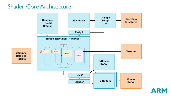
So far this is shaping up to be a banner year for SoCs. From a market perspective the mobile hardware space is still in a period of significant growth, but more importantly from a hardware point of view these products and especially the GPUs in these products have made significant strides in performance and in features. SoC GPUs will approach feature parity with desktop GPUs this year, and from a performance perspective they’re nearing the performance of the last-generation game consoles, a long-aspired goal given the “good enough” status attached to those devices.
Meanwhile at the same time that these products are maturing at a technical level, we’ve seen the various SoC firms mature at a professional level. The “wild west” days of SoCs have given way to mature markets of longer product cycles, longer product lives, and a more stable market overall. This both good and bad news for the various players in the SoC market as firms get squeezed out – SoC integrators such as TI and STMicroelectronics have been the first of such victims – but it also means that as companies become better established and more deeply entrenched, they can be more open about their projects and their products, and discuss them in greater detail than before without needing to be concerned about getting scooped by a competitor.
Here at AnandTech we’re particularly fond of doing architectural deep dives; our chance to talk to the people behind various processors and learn from them about how their products work and how they came together. Thanks to the maturation of the SoC market we’re finally getting a level of access in the SoC market that we haven’t had before, and in turn for the first time we get to tell the stories of the people behind these mind-bogglingly complex devices while better learning how they operate and as such how they compare. It’s admittedly a level of access we take for granted in the PC space, where companies such as Intel, AMD, and NVIDIA are regularly open, but it’s hard to contain our excitement about gaining this kind of access to the myriad of players in the SoC space.
This year then has been especially productive in that regard, and as of today it’s going to get even better. After we took a look at Imagination’s PowerVR Rogue architecture earlier this year, ARM contacted us and indicated that they would like to do the same; that they would like to take a seat at the “open architecture” table. To give us the access we need to discover how their GPUs work, and in turn tell you what we’ve learned.

To that end we’ve gladly let ARM pull up a seat, and today we’ll be taking our first in-depth look at ARM’s newest Mali SoC GPU architecture: Midgard. Now as with Imagination what we’re seeing today is most, but not all of the picture, as ARM has their secrets and they wish to keep some of them. But today we get to learn all about Midgard’s shader cores while also learning a thing or two about its pixel rendering pipeline, power optimizations, and other aspects of what makes Midgard tick. In other words, more than enough to keep us busy for one day.
But before we dive in we’d also like to quickly call attention to an Ask The Experts session we held with ARM’s Jem Davies, an ARM Fellow and VP of Technology in the Media Processing Division. While our deep dive is focusing on Midgard’s architecture, Jem has been answering all sorts of additional Mali-related questions, including business strategy and ARM’s views on GPU computing.
Finally, as this is the second article in our continuing series on SoC GPUs, we will be picking up from where we left off after our last article. While all of our articles are meant to be accessible to some degree, if you haven’t caught any of our previous articles I’d highly recommend our primer on how GPUs work for a quick overview of the technology before we dive into the nuts and bolts of ARM’s Midgard architecture.


66 Comments
View All Comments
toyotabedzrock - Friday, July 4, 2014 - link
Didn't imagine also buy from ATI? Maybe that is why they are concerned with patents?Kevin G - Saturday, July 5, 2014 - link
There likely is a cross licensing agreement in place. Literally to build any modern GPU a company has to cross license patents. It works out to be zero sum in that money isn't exchanged but one company can use the other's patents (and future patents) royalty free.This also puts a rather high barrier to entry in the market.
nolaviz - Thursday, July 3, 2014 - link
Ah, the history... I led the integration of MALI55 into Zoran's APPROACH-5C. Sweet memories :)skiboysteve - Thursday, July 3, 2014 - link
Very interesting. Complete 100% opposite of the AMD architecture.Also, the fact that they can power down shader cores and even individual ALUs makes this pure ILP and zero TLP architecture really shine. Because the compiler only needs to optimize work on an ALU level.... Not on a shader or wavefront level. So then based upon demand they just feed more or less of these ALU-optomized-packets of work into the GPU and power down the rest of the ALUs. It makes complete sense. Make each ALU independent, compile work on a per ALU basis, then scale your ALU utilization at run time... And also scale your chip portfolio on ALU count. Perfect scalability in price, performance and power combined with straightforward driver work.
Awesome!
rootheday - Thursday, July 3, 2014 - link
Transaction Elimination might work for "render to texture", where the texture is then used later in the scene, but it doesn't make sense to me for the final render target that is shown on the screen.. Typically your final render target is part of a swap chain with 2 or 3 different buffers. So the CRC computed for a tile in Frame N would need to match the CRC for frame N-2 (or maybe N-3), not N-1.EdvardS - Thursday, July 3, 2014 - link
So each buffer has its own CRC buddy attached to it - problem solved :-) Longer buffer chains just reduces you temporal coherency a bit.hexgrid - Thursday, July 3, 2014 - link
Relying on a 32bit hash for transaction elimination is a very bad idea. Assuming a normal distribution of hash results, the Birthday Paradox means you've got a better than 50% chance of collision if you have more than ~5000 items being hashed. The compartmentalized comparisons (it looks like they only compare against the same tile) means the collision rate will be lower, but there will be collisions, and in some cases they will look terrible.If there's a glitch, there's an excellent chance it will persist for a while. For example, let's say I'm bringing up a "pause" menu. If the title overlay of the pause menu happens to hash to the same value as the background that it replaced, that one tile of the pause menu title won't appear. Next frame, it still won't appear, because again the hash value hasn't changed. Until something happens to actually change the title or make it disappear, the glitch will persist.
The "fix" will be to do GUI overlays in translucency and keep the background animating somehow to prevent cache misses from sticking around, but it's an ugly hardware hack that will force software workarounds.
EdvardS - Thursday, July 3, 2014 - link
What if the CRC is 64 bit for each small tile? Quite overkill and very hard to break.mkozakewich - Sunday, July 6, 2014 - link
If the pause screen fades in, wouldn't that change the image data enough that it would generate entirely different CRCs for each frame until the animation ended?At any rate, my rule of thumb would be that if it doesn't happen more often than a keyframe is dropped in a video, it'll be fine.
Krysto - Thursday, July 3, 2014 - link
I'd like you guys to do more 30x GFX loops, that how whether these GPU's only prop up high numbers at first, but then quickly get throttled. From what I noticed Imagination is the only one that doesn't throttle in that test. But I'm curious to see if K1 and T760 do.