Imagination's PowerVR Rogue Architecture Explored
by Ryan Smith on February 24, 2014 3:00 AM EST- Posted in
- GPUs
- Imagination Technologies
- PowerVR
- PowerVR Series6
- SoCs
Background: How GPUs Work
Seeing as how this is our first in-depth architecture article on a SoC GPU design (specifically as opposed to PC-derived designs like Intel and NVIDIA), we felt it best to start at the beginning. For our regular GPU readers the following should be redundant, but if you’ve ever wanted to learn a bit more about how a GPU works, this is your place to start.
GPUs, like most complex processors, are composed of a number of different functional units responsible for the different aspects of computation and rendering. We have functional units that setup geometry data, frequently called geometry engine, geometry processors, or polymorph engines. We have memory subsystems that provide caching and access to external memory. We have rendering backends (ROPs or pixel co-processors) that take computed geometry and pixels to blend them and finalize them. We have texture mapping units (TMUs) that fetch textures and texels to place them within a scene. And of course we have shaders, the compute cores that do much of the heavy lifting in today’s games.
Perhaps the most basic question even from a simple summary of the functional units in a GPU is why there are so many different functional units in the first place. While conceptually virtually all of these steps (except memory) can be done in software – and hence done in something like a shader – GPU designers don’t do that for performance and power reasons. So-called fixed function hardware (such as ROPs) exists because it’s far more efficient to do certain tasks with hardware that is tightly optimized for the job, rather than doing it with flexible hardware such as shaders. For a given task flexible hardware is bigger and consumes more power than fixed function hardware, hence the need to do as much work in power/space efficient fixed function hardware as is possible. As such the portions of the rendering process that need flexibility will take place in shaders, while other aspects that are by their nature consistent and fixed take place in fixed function units.
The bulk of the information Imagination is sharing with us today is with respect to shaders, so that’s what we’ll focus on today. On a die area basis and power basis the shader blocks are the biggest contributors to rendering. Though every functional unit is important for its job, it’s in the shaders that most of the work takes place for rendering, and the proportion of that work that is bottlenecked by shaders increases with every year and with every generation, as increasingly complex shader programs are created.
So with that in mind, let’s start with a simple question: just what is a shader?
At its most fundamental level, a shader core is a flexible mathematics pipeline; it is a single computational resource that accepts instructions (a shader program) and executes it in order to manipulate the pixels and polygon vertices within a scene. An individual shader core goes by many names depending on who makes it: AMD has Stream Processors, NVIDIA has CUDA cores, and Imagination has Pipelines. At the same time how a shader core is built and configured depends on the architecture and its design goals, so while there are always similarities it is rare that shader cores are identical.
On a lower technical level, a shader core itself contains several elements. It contains decoders, dispatchers, operand collectors, results collectors, and more. But the single most important element, and the element we’re typically fixated on, is the Arithmetic Logic Unit (ALU). ALUs are the most fundamental building blocks in a GPU, and are the base unit that actually performs the mathematical operations called for as part of a shader program.
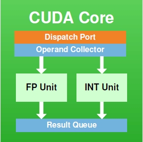
An NVIDIA CUDA Core
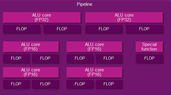
And an Imgination PVR Rogue Series 6XT Pipeline
The number of ALUs within a shader core in turn depends on the design of the shader core. To use NVIDIA as an example again, they have 2 ALUs – an FP32 floating point ALU and an integer ALU – either of which is in operation as a shader program requires. In other designs such as Imagination’s Rogue Series 6XT, a single shader core can have up to 7 ALUs, in which multiple ALUs can be used simultaneously. From a practical perspective we typically count shader cores when discussing architectures, but it is at times important to remember that the number of ALUs within a shader core can vary.
When it comes to shader cores, GPU designs will implement hundreds and up to thousands of these shader cores. Graphics rendering is what we call an embarrassingly parallel process, as there are potentially millions of pixels in a scene, most of which can be operated in in a semi-independent or fully-independent manner. As a result a GPU will implement a large number of shader cores to work on multiple pixels in parallel. The use of a “wide” design is well suited for graphics rendering as it allows each shader core to be clocked relatively low, saving power while achieving work in bulk. A shader core may only operate at a few hundred megahertz, but because there are so many of them the aggregate throughput of a GPU can be enormous, which is just what we need for graphics rendering (and some classes of compute workloads, as it turns out).
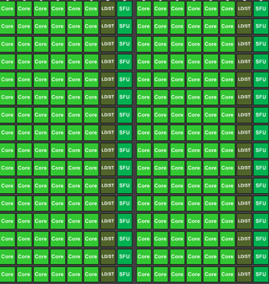
A collection of Kepler CUDA cores, 192 in all
The final piece of the puzzle then is how these shader cores are organized. Like all processors, the shader cores in a GPU are fed by a “thread” of instructions, one instruction following another until all the necessary operations are complete for that program. In terms of shader organization there is a tradeoff between just how independent a shader core is, and how much space/power it takes up. In a perfectly ideal scenario, each and every shader core would be fully independent, potentially working on something entirely different than any of its neighbors. But in the real world we do not do that because it is space and power inefficient, and as it turns out it’s unnecessary.
Neighboring pixels may be independent – that is, their outcome doesn’t depend on the outcome of their neighbors – but in rendering a scene, most of the time we’re going to be applying the same operations to large groups of pixels. So rather than grant the shader cores true independence, they are grouped up together for the purpose of having all of them executing threads out of the same collection of threads. This setup is power and space efficient as the collection of shader cores take up less power and less space since they don’t need the intelligence to operate completely independently of each other.

The flow of threads within a wavefront/warp
Not unlike the construction of a shader core, how shader cores are grouped together will depend on the design. The most common groupings are either 16 or 32 shader cores. Smaller groupings are more performance efficient (you have fewer shader cores sitting idle if you can’t fill all of them with identical threads), while larger groupings are more space/power efficient since you can group more shader cores together under the control of a single instruction scheduler.
Finally, these groupings of threads can go by several different names. NVIDIA uses the term warp, AMD uses the term wavefront, and the official OpenGL terminology is the workgroup. Workgroup is technically the most accurate term, however it’s also the most ambiguous; lots of things in the world are called workgroups. Imagination doesn’t have an official name for their workgroups, so our preference is to stick with the term wavefront, since its more limited use makes it easier to pick up on the context of the discussion.
Summing things up then, we have ALUs, the most basic building block in a GPU shader design. From those ALUs we build up a shader core, and then we group those shader cores into a array of (typically) 16 or 32 shader cores. Finally, those arrays are fed threads of instructions, one thread per shader core, which like the shader cores are grouped together. We call these thread groups wavefronts.
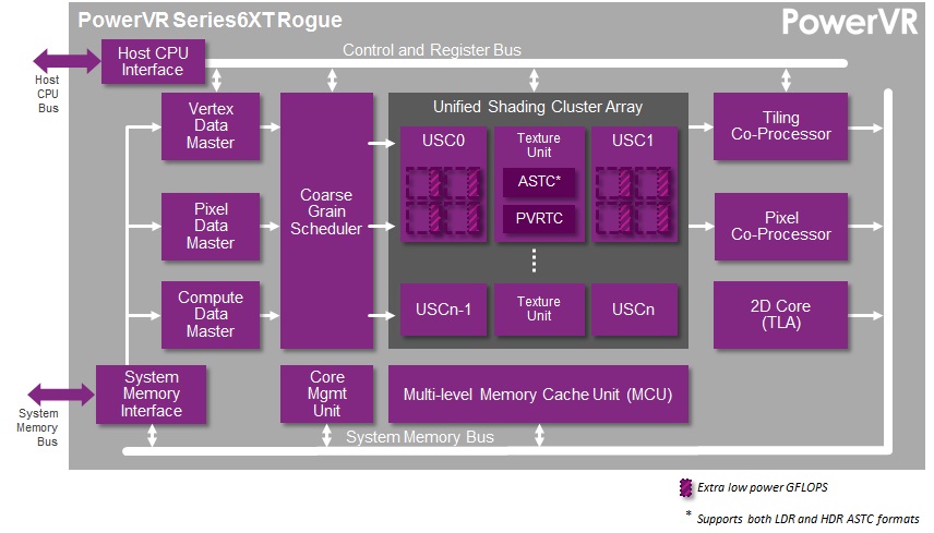
And with that behind us, we can now take a look at the PowerVR Series 6/6XT Unfied Shading Cluster.


95 Comments
View All Comments
jjj - Monday, February 24, 2014 - link
Far from ideal timing with so many news around, guess i'll have to read it after MWC.rpg1966 - Monday, February 24, 2014 - link
Thank you for sharing.Mondozai - Monday, February 24, 2014 - link
The most important part is what Anand highlighted from this walkthrough; namely that the Rogue series has a chip that is on equal balance if not even stronger than Tegra K1.Poor Nvidia.
Sabresiberian - Monday, February 24, 2014 - link
That remains to be seen - but it does appear to be competitive at this point. We also don't know what the entire Denver+K1 package will do.What kind of surprises me about K1 though is that Maxwell has already been released for the desktop. I would think "M1" (to guess at a name) would be the architecture to build on in the next year.
dragonsqrrl - Monday, February 24, 2014 - link
Uhhh no it doesn't. The article failed to mention this important piece of information, but you realize the 6XT series probably won't come to market before 2015 right? Likely 2H 2015 according to an earlier article published here on Anandtech.grahaman27 - Monday, February 24, 2014 - link
Interesting. Which article mentioned that? Would you mind linking me to it?I can't find an expected release date for this chip anywhere.
dragonsqrrl - Tuesday, February 25, 2014 - link
That's because there is none. It was an estimate given by Ryan Smith based on prior Imagination GPU announcements, and the time it usually takes chipmakers to integrate the design and bring a device to market."Finally, while Imagination doesn’t provide a timeframe for consumer availability (since they only sell designs to chipmakers), based on the amount of time needed to integrate these designs into new products and then get those products in the hands of consumers, we should be looking at a timetable similar to the original Series6 designs. In which case Series6XT equipped SoCs would start appearing in 2015, likely in the latter half."
http://www.anandtech.com/show/7629/imagination-tec...
michael2k - Tuesday, February 25, 2014 - link
Really? You don't think their biggest customer, Apple, which has shown the ability to beat an entire industry to market by almost a year (64 bit ARMv8) and one of the first PVR6 customers to market as well? Anand though it would be 2014 when PVR6 would show up to market, and the A9600 that was supposed to show up in 2013 never did (Apple's A7 did though!)So why do you rule out the real possibility that the Apple A8 would ship with a 6XT this year?
dragonsqrrl - Tuesday, February 25, 2014 - link
I don't know, ask Ryan Smith.My theory for the ~18 month estimate is that it's about how long Apple took to integrate and bring their current series 6 GPU to market in the A7. I suppose if any company had the resources to accelerate that schedule, it would be Apple. But then the question becomes why and does it make sense? There will be faster Series 6 SKU's available for the A8 in the interim.
stingerman - Wednesday, February 26, 2014 - link
But don't forget, Apple has been involved in this design long before Imagination's public reveal. In fact, Apple informed Imaginations design with their real world experience and their own needs. I always expect Apple to get a 6 to 12 month lead. And, Apple has shown themselves to put a very high value on their SoC GPU leadership.