An Introduction to Semiconductor Physics, Technology, and Industry
by Joshua Ho on October 9, 2014 3:00 PM EST- Posted in
- Semiconductors
- CMOS
- Physics
- Industry
- Technology
Improving Transistor Performance
While it's impossible to predict what the future will hold, it's relatively easy to see what trends will take place in the near future to keep Moore's law alive. For example, instead of using dual or tri gate technologies (FinFET), it's reasonable to expect that gate-all-around (GAA) will become the next step in the evolution of transistor shapes. However, it's currently not clear when this would reach mass production, if ever.
Currently, experimental GAAFETs have only existed for around eight years. For reference, FinFETs were first made in 1999. It took around a decade and a half for any such 3D transistor to reach mass production. By continuing to scale to higher k dielectrics for the gate, lower k dielectrics between interconnects, lower resistance metals for interconnects, and even better strain engineering, we will continue to see the scaling of CMOS technology.
CNFET / Joerg Appenzeller
Unfortunately, all of these can only go so far. Fundamentally, there will be a point where silicon-based transistors cannot scale any further. Gate oxides, channel lengths, and other critical dimensions can only shrink so much before either resistance is too high or a myriad of other effects render smaller sizes infeasible.
The next step is almost impossible to predict. Perhaps graphene will take the place of silicon, but graphene currently is impossible to mass-produce and is a semi-metal, which means that it inherently lacks a band gap, although it's possible to create one. While it's been shown that semi-metal transistor logic is possible, it's currently in the very early stages and Boolean logic may be impossible with graphene. Phosphorene has promise as a semiconductor replacement for silicon, but it's similarly impossible to mass produce. Phosphorene-based FETs are still in the exploratory stages, with no actual transistor created yet.
TFET Lateral Structure / Jteherani / CC BY SA
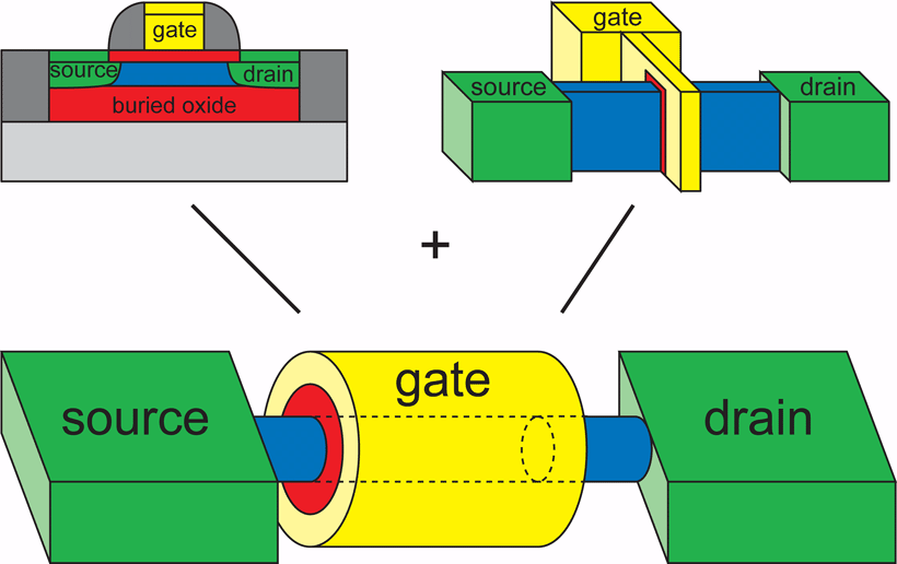
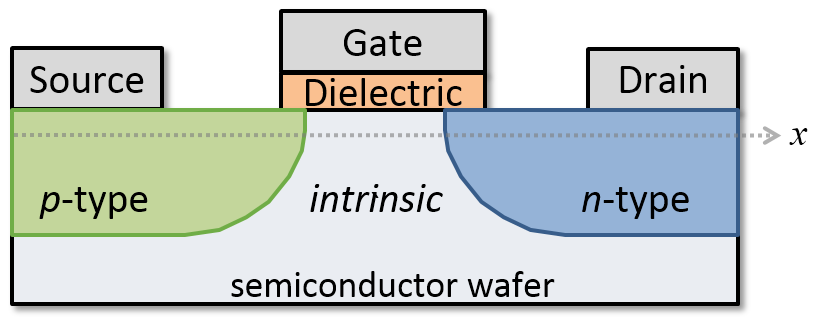
Outside of material changes, the working mechanism of the transistor itself may change. One promising candidate right now is the tunnel field effect transistor, which relies on band to band tunneling rather than the traditional inversion layer generation for current flow. This is similar to leakage that occurs from halo doping, which results from the conduction band of the channel material aligning with the valence band of the source or drain material. As seen by the photo above, this type of transistor has an undoped body and the source/drain are of opposing types. The gate structure is unchanged from previous MOSFETs. In practice, such a transistor structure has a much higher rate of current increase per unit of voltage.
Final Words
It's been a long road, but let's quickly go over the topics covered in this article. We started with a description of semiconductor physics, then moved to the basics of MOSFETs and CMOS. Once we understood how MOSFETs work in CMOS to create logic, we moved on to the actual fabrication process of these transistors in a chip.
After all of this, we discussed how companies have increased the resolution of the fabrication process to make ever smaller transistors, and we continued by looking at how companies have increased transistor performance despite significant engineering challenges. Then we briefly covered what the future may hold for improving device performance and continuing to improve the lithography process to continue making smaller transistors.
But there is far more to be done, as literally everything we write about at AnandTech depends upon ever faster, smaller, and more efficient transistors packed as tightly as possible. Without this continued innovation, the PC, smartphone, and wearables that we see today would be impossible to make. However, continuing the scaling that we have seen within the past decades will require more ingenuity and resources than ever before to continue pushing the limits of what's possible.
Normally, we would end things here, but this time I'd like to end by thanking everyone that has helped make this article possible. It has taken weeks of research and asking questions to get to this point, and I'm sure that without help it would have taken months. Out of the many that have helped, I'd like to specifically thank Chenming Hu, a professor in the graduate school at UC Berkeley and the lead researcher in FinFET and UTB-SOI/FD-SOI, for taking the time to help clarify the reasons for SOI and FinFET. I'd also like to thank Gerd Grau, a doctoral candidate in the graduate school at UC Berkeley, and Intel's TMG for answering all kinds of questions about solid state physics in general.


77 Comments
View All Comments
toyotabedzrock - Tuesday, October 14, 2014 - link
It sounds like electron beam is the best path forward but I have a feeling the bean counters will push for using the nano method because it would create "efficiencies" that shareholders would love. I don't see any mold at that feature size being reusable. It seems like we are approaching a size where we will be lowering energy efficiency due to leakage and limitations it clock speed.I remember reading about a new type of transistor Intel was working on that required much less voltage, that would be a good next step.
Kidster3001 - Wednesday, October 29, 2014 - link
That would be NTV or Near Threshold Voltage. Basically, requires a lot less energy to turn transistors On and Off, which just happens to be the only time they consume energy (not counting leakage)victorson - Tuesday, October 14, 2014 - link
Great work, Joshua, I still find it a bit too challenging of a read, especially at the chemistry level, but will definitely chew through this in a couple of attempts.Marvin Wankerstein - Sunday, October 19, 2014 - link
First - very nice article. It was nice to read such a good summary of much of my graduate school days.I was rather disappointed that you did touch on what a stepper is and what the term "stepping" means since I see it so frequently misused.
Regardless, I enjoyed the article very much.
LapX - Tuesday, October 28, 2014 - link
I want to major in electrical engineering (Ihave 7 years to go before I'm finished) and I find this article very interesting but I still can't figure out how you can create logic with the transistors or how do they switch from on to off, is it switching itself when the current is too low/high if I undestood correctly?campbbri - Wednesday, October 29, 2014 - link
Thank you for the great article!SanX - Sunday, May 24, 2015 - link
OK, take 50nm, with doublepatterning 25. How they get 14 and even 10nm? That needs something else. You can not make 10nm line with 20x longer wavelength