Samsung SSD 850 Pro (128GB, 256GB & 1TB) Review: Enter the 3D Era
by Kristian Vättö on July 1, 2014 10:00 AM ESTAnandTech Storage Bench 2011
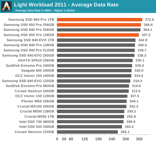
Back in 2011 (which seems like so long ago now!), we introduced our AnandTech Storage Bench, a suite of benchmarks that took traces of real OS/application usage and played them back in a repeatable manner. The MOASB, officially called AnandTech Storage Bench 2011 - Heavy Workload, mainly focuses on peak IO performance and basic garbage collection routines. There is a lot of downloading and application installing that happens during the course of this test. Our thinking was that it's during application installs, file copies, downloading and multitasking with all of this that you can really notice performance differences between drives. The full description of the Heavy test can be found here, while the Light workload details are here.
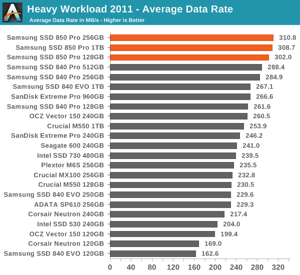
The dominance continues in our 2011 Storage Benches. The 840 Pro was already the fastest drive in both suites, so it does not come as a surprise that the 850 Pro takes the lead.


160 Comments
View All Comments
emvonline - Tuesday, July 1, 2014 - link
is the die size for the NAND chip 67mm^2? I assumed you measured it (pretty easy to do). I would think it would be much larger than thatGigaplex - Tuesday, July 1, 2014 - link
It's difficult to measure the die when multiple of them are on the same package.emvonline - Tuesday, July 1, 2014 - link
send me the package... I promise to have exact die size in a week ..... TEM cross sections in two weeks :-)Kristian Vättö - Tuesday, July 1, 2014 - link
Send me an email at kristian@anandtech.com and let's work this out :)extide - Tuesday, July 1, 2014 - link
Yes, 67mm^2, but remember that is 32 "deep"emvonline - Tuesday, July 1, 2014 - link
@extide: so you measured the die to be 67mm^2? how was this measured ? CSAM? XRAY? that seems odd to use such a small dies for SSD. and that would make it even smaller cell size than the one at ISSCC since it was 134 for a 128Gbit with 24 layers (periphery doesnt shrink as fast with lower density)Kristian Vättö - Tuesday, July 1, 2014 - link
No I didn't because I don't have the equipment to do that. The method I used to calculate the die size is explained on the fifth page of the review:http://www.anandtech.com/show/8216/samsung-ssd-850...
I'm not claiming that it is an accurate figure, hence the "~" sign in front of it. However, Samsung wouldn't disclose the die size when I asked them during the Q&A, so at this point I don't know for sure. However, I have a picture of the 32-layer wafer and once I get back home I'll do the math of the wafer to figure out the exact die size.
emvonline - Tuesday, July 1, 2014 - link
Got it thanks. I am mainly wondering about redundancy, extra blocks and ECC overhead.drwho9437 - Tuesday, July 1, 2014 - link
The micrograph you say is an "x-ray", is almost certainly a transmission electron microscopy image. Given the oxides are light it is a bright field image. It could technically be a SEM image but the resolution is a bit to high, so it most likely is a STEM image with a bright field detector.GTVic - Tuesday, July 1, 2014 - link
Perhaps time should be added as a cost efficiency factor. Presumably the die has to stay in the process much longer due to all the layers being added one at a time.